Archive for the ‘Hacking’ Category

Winner, Name that Ware May 2011

Wednesday, June 22nd, 2011

The Ware for May 2011 is an Intel SSDSA2CW300G3 300 GByte solid state drive.

Here’s the complete scans of the front and back of the PCB, since I have ’em:

I recently upgraded my trusty T61p laptop to a T520, and decided that I’d also drop in a pair of SSDs. The T520 is a great machine, btw. I have one 300 GB Intel SSD in the main slot, and a 128 GB Samsung SSD in the Ultrabay. My old T61p had a single 256 GB Samsung SSD, which replaced a Crucial SSD that failed within hours of installation.

After the false start with the Crucial SSD, I was wary of the reliability of these devices. Now, I’m pleased to say that after a year and a half of heavy use the Samsung still works well, although the write times have gotten quite bad. Hence, the dual-SSD setup: mostly static files go on the Intel SSD, and the Samsung SSD gets the big temp/scratch files, with the intention that it will be replaced every year without having to re-image the laptop.

This past month’s ware was an easy one to guess, but I can’t make all of ’em tough; there’s just too many smart readers out there. I’ll just go with the first responder as the winner, Ty_a. Congrats! email me for your prize.

Name that Ware May 2011

Monday, June 6th, 2011

The ware for May 2011 is shown below. Click on the image for a much larger version.

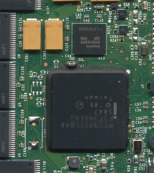
I’ve cropped out about 70% of the circuit board, but I think there are still ample details remaining to enable you to guess this one reliably, probably down to the model and part number. Have fun!

I think it’s interesting how the epoxy underfill on the center BGA has depressions in it to reveal the test points underneath (I think it’s also heartening that they elected to use underfill). I wonder how this was accomplished. Underfill is chosen specifically to have good wetting properties, and it cures hard. So, the only way I can think of making those depressions in to attach a jig that’s present while the underflow cures. Seems like a lot of effort for two test points, one of which could be easily moved to a zone outside of the underfill’s reach.

Also, to readers unfamiliar with underfill — a number of people have shown me boards with underfill on them, and have incorrectly identified the underfill as an anti-tamper security measure. While underfill does make it harder — although not impossible — to remove the chip, the technology was not developed primarily for security. Underfill exists because BGAs have a tendency to delaminate and crack off of the PCB, resulting in reliability issues over time. The mechanism can be due to vibration, shock, flexing, or thermal cycling. Thermal cycling is a natural result of warming and cooling due to turning the device on and off. The chip package and the mating board grow and shrink at different rates due to different coefficients of thermal expansion. This causes the solder balls to undergo a mechanical stress that can eventually lead them to shear or crack. The Xbox360, for example, lacks underfill on the GPU, and this could be a contributing factor to the infamous “Red Ring of Death” issue.

Underfill is quite standard on all manner of gadgets that can be carried about, flexed, dropped, and/or subject to vibration. However, underfill is devilishly tricky to apply correctly. If air pockets are trapped during the application of the underfill, it can actually make the problem worse by concentrating all the stress in the air pockets. Hence, the epoxy used for underfill in uniquely engineered and (if your factory is doing it right) applied by a robot to ensure that no air is trapped in the gap underneath as it flows underneath the soldered-down BGA. Which leads to why I find the test points poking through the underfill to be interesting, because the epoxy should have flown right over the bumps, even if it was temporarily displaced for testing prior to curing; and after curing, the epoxy should be rock-hard and impenetrable to test probes.

Winner, Name That Ware March 2011

Monday, June 6th, 2011

The Ware for March 2011 is a Vista 1600 Environmental Radiation Probe by International Medcom. It was a ware that I snapped a photo of while in Tokyo in April. Christian Vogel is the winner of March 2011, congrats, email me for your prize! While nophead had the right answer first, Christian wins for depth and insight of analysis.

Sorry I’m running a bit late on name that ware the past couple of months. Things have been hopping. Right now is “high season” in the consumer electronics design industry — unlike the movies, Santa’s little elves don’t build your gadgets the week before Christmas — it’s all happening right about now in Asia.

Name That Ware April 2011

Sunday, May 8th, 2011

The Ware for April 2011 is shown below, click on the image for a much larger version:

Enjoy!

Winner, Name that Ware March 2011

Sunday, May 8th, 2011

I’ve had some good fun with FPGAs over the past month and I was curious to see what was inside the JTAG programming box; thus, the Ware for March 2011 is the Xilinx platform cable USB II. Here’s a full image without the part number redactions. The winner of last month’s competition is Fiach Antaw, please email me to claim your prize.

Incidentally, the Xilinx ISE tools have come a loooong way since I started using them back in the mid-90’s while I was an undergrad at MIT (and fwiw, Xilinx’s university sponsorship program worked on me hook, line and sinker: to this day I remember their donations of parts & tools, and I still exclusively use Xilinx FPGAs). The most recent addition to the design tools suite is Chipscope, which enables you to instantiate a virtual logic analyzer inside the FPGA to analyze your design in-situ. It’s very powerful and makes short work of debugging some difficult problems, particularly ones involving timing conditions that are hard to replicate in simulation.