IRIS (Infra-Red, in-situ) is a multidisciplinary project I’m developing to give people a tangible reason to trust their hardware.
Above: example of IRIS imaging a chip mounted on a circuit board.
When I set out to research this technique, there were many unknowns, and many skills I lacked to complete the project. This means I made many mistakes along the way, and had to iterate several times to reach the current solution.
Instead of presenting just the final solution, I thought it might be interesting to share some of the failures and missteps I made along the way. The propensity to show only final results can make technology feel less inclusive: if you aren’t already in the know, it’s easy to feel like everything is magic. Nothing can be farther from the truth.
This short “sidebar” post will wax philosophical and discuss my general methods for learning and exploration; if you have no interest in this topic, you can safely skip this post.
The Rule of Three
When I have no way to derive how many iterations it will take to get something right, I use the “rule of three”: generally, you can get somewhere interesting with three iterations of a methodical process. The rule of three has roots in the observation many natural phenomena can be described with relationships based on the natural logarithm, e. In particular, diffusive processes – that is, progress toward a goal that is driven by random walks over a concentration gradient – have shapes and time constants governed by this relationship. As a corollary it matters less the exact nature of the process, and more the magnitude and proximity of the realizable incentives to get it right.
Such processes tend to get “63% of the way there” in the first interval, “86% of the way there” in the second interval, and “95% of the way there” by the third interval (these percentages correspond to inverse powers of e, that is: 63% ≈ 1 – e-1, 86% ≈ 1 – e-2, etc…). You can’t iterate to perfection, but 95% of the way there is usually good enough. So when I can’t find a better analysis to guide a process, I’ll apply the “rule of 3” to everything from project management for a complex system, to how many times I rinse a dish rag before I hang it to dry.
Meta-knowledge: Knowing what You Know
When it comes to planning a big project like IRIS, a realistic self-assessment improves my ability to estimate time and resource requirements; the rule of three only works if you’re realistic about what you can achieve with every iteration.
Thus, I have developed a series of criteria to keep myself grounded, and periodically I take some time to reflect and correct my behavior if it is out of line.
Here is my self-assessment criteria, presented as a series of statements I can make about my knowledge, followed by a set of tests I might use to prove the statement.
I am ignorant of it: the concept does not exist in my consciousness; there’s an instinct to reject the possibility of its existence, especially if it is adjacent to something I already know well. The path to knowledge starts with recognizing ignorance; learning the smell of my own ignorance (that is, the instinct to reject or be incredulous) helps me get over this barrier faster.
I am aware of it: I’ve heard enough about it that I can throw the term around in the right context and impress someone who hasn’t heard of it.
I know of it: I’ve seen others do it, read some articles or papers about it, perhaps even played with a toy version of it and/or correctly answered basic questions about it.
Everyone is different, but this is roughly the level of knowledge I felt I had when I finished my basic undergraduate-level courses in university.
I have tried it out: did a small “original” project with it, and it seemed to go OK. This is the point where it’s easy to fall into the trap of knowing enough to be dangerous, but not realizing it.
This is around the point I felt I got to after completing some thesis-level projects in university.
I know it: did at least two projects with it, one of which I struggled to finish, because I hit a limit of the example code, API, or physics
This is roughly where I felt when I was as a junior professional in my first jobs out of college.
I know it well: extended it with a previously unknown aspect, or built a version of it from near first-principles; can teach it to others, but pupils still come away overwhelmed by jargon. Usually requires at least one several-month period of not touching it, and then coming back to it before I can reach the next stage
I have mastered it: knowing what I don’t know about it, and what it might take to figure out the missing bits; can correctly identify which problems it can be used to solve, and effectively solve them; able to use it as a reference to explore other less-known things; can readily extend it to meet other people’s needs; can offer a lucid and compact explanation of the topic to a beginner, without relying on jargon.
This is roughly what I would expect out of a senior professional or professor.
I am overfitting it: using it to solve everything, and everything is solvable with it; learning new things is harder and riskier relative to converting all the problems into something solvable with it – so I stop learning new things and spend more of my time converting all problems into its domain. This is the point at which everything looks like a nail because you’ve got a really nice, fancy hammer and you can swing it like nobody else can.
Overfitting can happen at any stage of learning, but it tends to happen whenever you become the most skilled within a given peer group. It’s avoidable, but is often a terminal state of learning. Overfitting can prevent forward progress in other skills, because it can seem like there is no need to master any other technique since you’re already “the smartest person in the room”.
I find that the final stages of learning are a constant tension between overfitting and asymptotically approaching mastery; there is no clear answer as to when I’m overfitting or when I’m just judiciously applying a well-worn tool to a job. However, as a matter of habit, when I start to feel too comfortable with a tool or technique, I try to force myself out of my comfort zone and try something new, just to make sure I’m not overfitting.
There is a cost to this, however, since it almost always means passing up easy money or fame to make the time to explore. An excellent way to break the overfitting cycle is to create art. Art is a safer space for exploration; even technical failures, if sufficiently spectacular, may have artistic merit. I also learn a lot when I collaborate with artists, because they often see aspects of familiar topics that I’ve been blind to my entire life.
Working within my Limitations
Significantly, progress past the “know it well” stage often requires me to take a several month break from doing anything with the topic or tool. During this time, all my short-term memory of the subject is lost, so I have to re-acquire the knowledge when I return to the topic. Re-learning from experience is an important step because I get a fresh look on the topic. Because I’m already somewhat familiar with things, I have the surplus cognitive capacity to put everything into context, while having the awareness to identify and break bad habits.
This cool-down period on learning puts a fundamental cap on the rate at which I can learn any single topic, but, the process of forgetting is aided by rotating through other skills and learning other things. I can use this to my advantage to learn several things in parallel. As a result, I generally try to have at least two projects running at the same time, each exercising a different set of skills. For example, most recently I have been alternating between maintaining the Xous OS (Rust programming), designing IRIS (mechanical design), and designing the next-generation Precursor (chip design).
At least for me, another important aspect is also knowing when to stop learning. You don’t need to be a master of everything (if your goal is to build a thing and deliver it on time). The trick is to learn just enough to get the job done correctly. Since time is a limited resource, overlearning can be as problematic as overfitting. My usual rule is to learn enough to get the job done, and then just enough more to be aware of a few crucial things that I might be missing. If none of these things have a substantial impact on the outcome of the project, it’s time to move on.
In the next post, I’ll describe the process of creating a light source for IRIS as a case study of this self-assessment methodology in action.
A goal of mine is to give everyday people tangible reasons to trust their hardware. Betrusted is a multi-year project of mine to deliver a full-stack verifiable “from logic gates to Rust crates” supply chain for security-critical applications such as password managers. At this point, many parts of the project have come together: Precursor is an FPGA-based open hardware implementation, and it runs Xous, our Rust-based microkernel message-passing OS. I currently use my Precursor on a daily basis with the “vault” application loaded to manage my passwords, TOTP tokens, and FIDO/U2F logins.
However, Precursor is expensive, because FPGAs are expensive. The device could be much cheaper with a dedicated security chip, but then we have no reason to trust these chips – security chip vendors don’t facilitate any form of user-side inspection, so we can’t tell if we have real or fake security chips in our device.
Kind of defeats the purpose, if you ask me.
Last March, I introduced the concept of Infra-Red, in situ (IRIS) inspection of silicon in a blog post and an arXiv paper. My hope has been that IRIS, plus some circuit-level scans and mathematical methods, could be the missing link that allows us to transition from our expensive FPGA-based Precursor solution, to a more pocketbook-friendly ASIC-based solution.
At the time when I released the initial paper, every picture was manually composed and focused; every sharp image was cherry-picked from dozens of fuzzy images. It was difficult to reproduce images, and unsuitable for automatically tiling multiple images together. The technique was good enough for a demo, but shaky as a foundation for full-chip verification.
Over the past year, I’ve refined the technique and implemented a fully automated system that can robustly and repeatably image whole chips at micron-scale resolution in a matter of minutes. The idea is not for everyone to have one of these robots in their home (but how cool would that be!); rather, the idea is that most users could utilize an inexpensive but somewhat fiddly setup and compare their results against reference images generated by the few users like me who have fully automated systems.
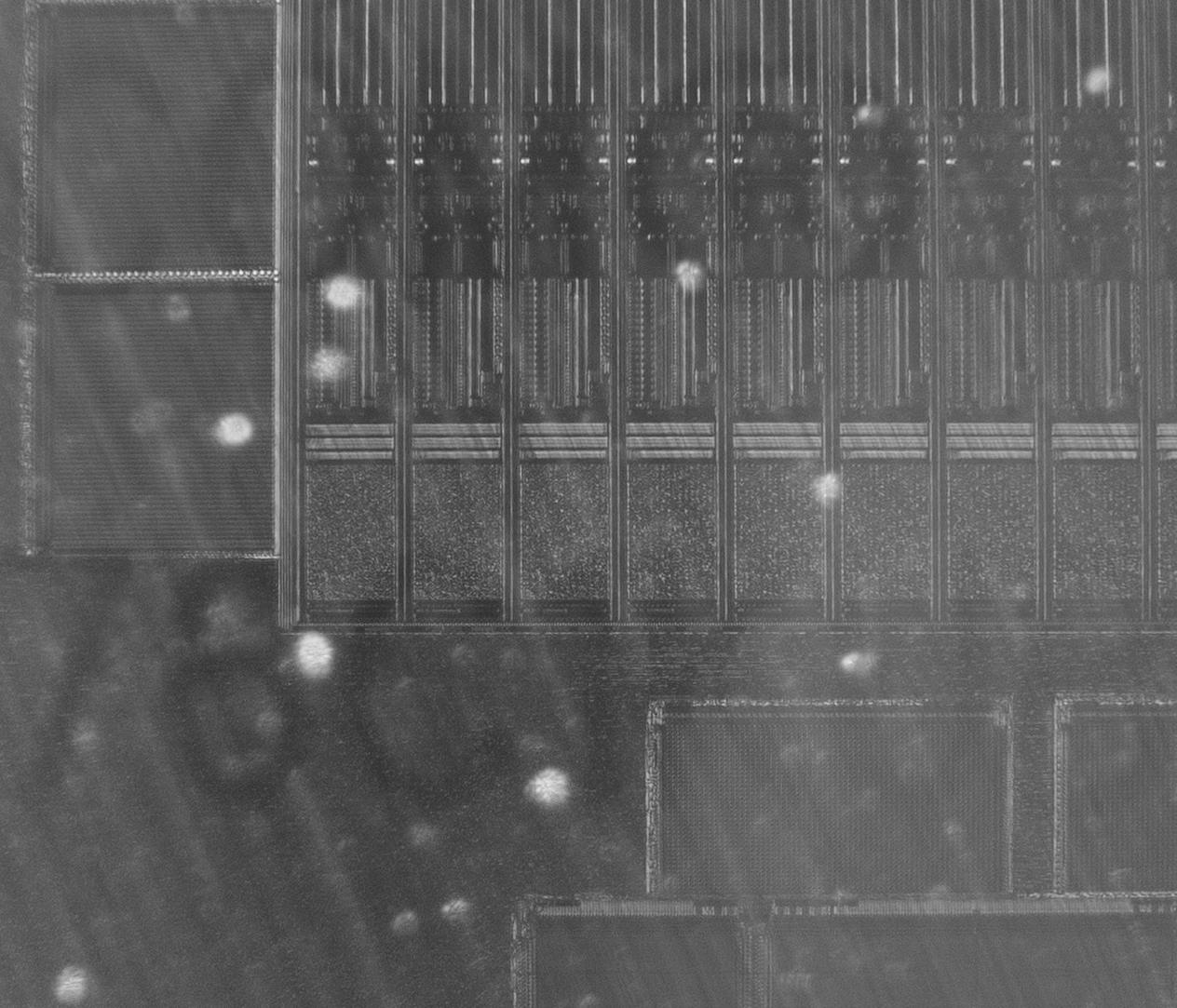
Here’s an example of the MPW7 run on SKY130A, courtesy of Matt Venn, imaged using my automated IRIS machine:
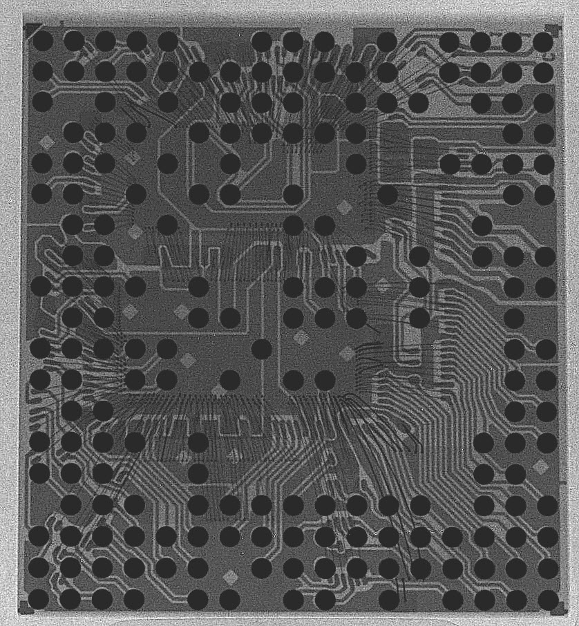
The above is just a thumbnail; click on the image to zoom into and browse the full-resolution version at siliconpr0n.org (and check out my collection on that server for some more full-chip IRIS images). Each of the mottled dots in the lighter-shaded rectangles in the image corresponds to a logic gate, flip flop, or a “fill cell” (dummy transistors wired up as decoupling capacitors). To create the image, I just had to tell the machine where three corners of the chip are, and it automatically focuses and scans the full area. A script then post-processes the tiles into the fully-composed image you see here.
A broad goal of the project is to democratize silicon imaging and improve the state of the art in hardware verification. This is an area where simply popularizing silicon imaging can move the needle on security for everyone, because a credible threat of being caught reduces the incentive for adversaries to invest in expensive Trojan-implantation capabilities.
The good news is that the project is now at a state where, over the next couple of months, I can share a series of posts that detail the methodology used to develop the automated IRIS system, as well as document the construction of the device.
To kick things off, I’m going to start with a review of the current state of the art in hardware verification.
Review: Current State of the Art in Hardware Verification
Is my computer trustworthy? How do I know it was built correctly, and will execute my instructions faithfully? These are the questions that hardware verification aims to answer.
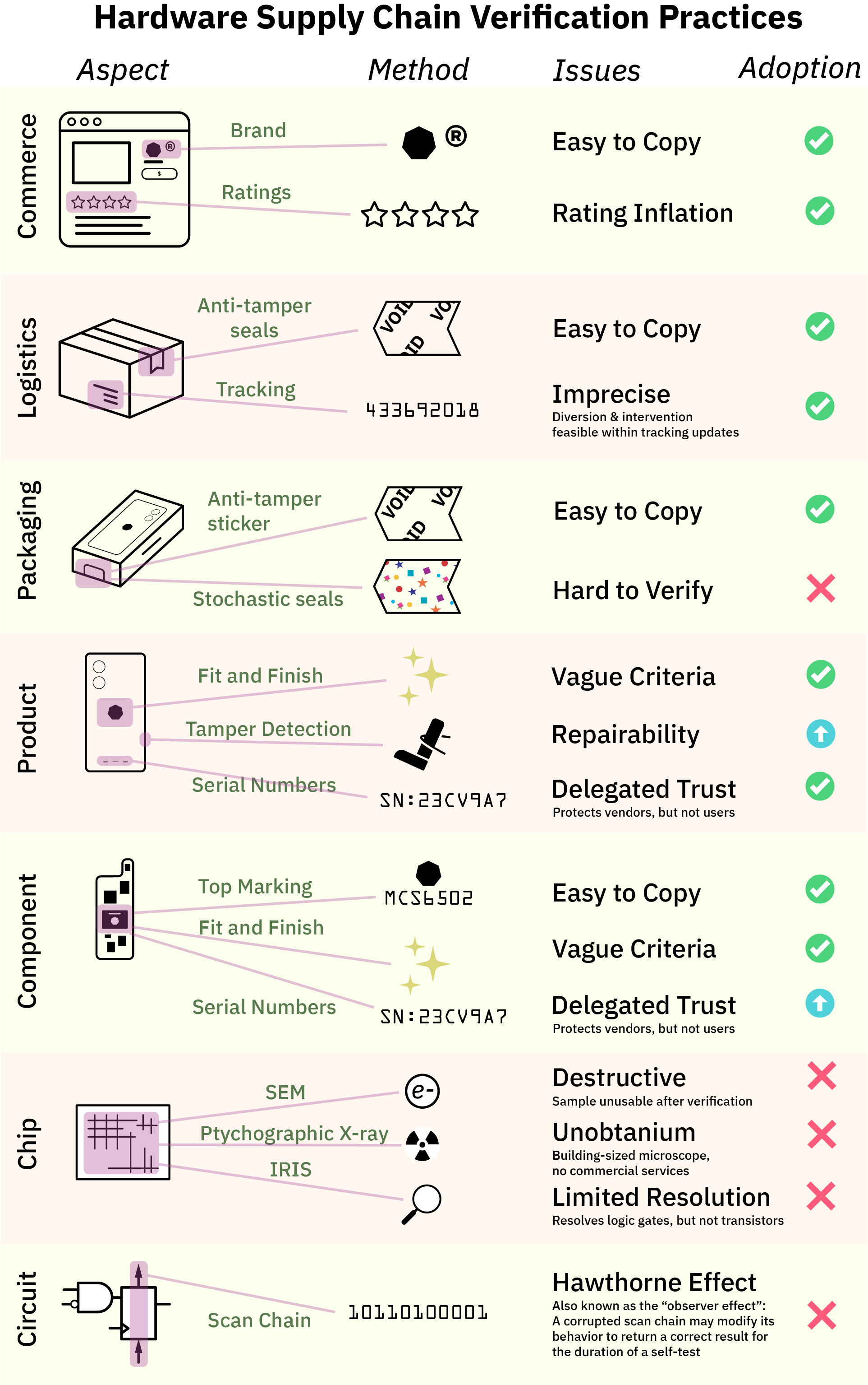
Hardware verification happens at every level of the supply chain. Let’s start with the relatable, every-day problem of how do I pick a piece of hardware to buy, and from there dive all the way down to esoteric topics such as verifying the circuits and devices that make up the hardware itself.
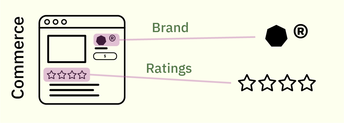
Consumers shopping for a computer rely principally on reputation mechanics to make choices: is the manufacturer a reputable brand? And how do my peers rate it?
Many of us can relate to how these mechanisms can fail. Ratings can be inflated by purchasing fake reviews, and stores can sell counterfeit brand goods. “Surely, this is just a problem of the retail market”, one might think. Once we’ve waded through the swamp of advertisements and on-line storefronts, the powers that be ought to ensure the device we ordered is the device we get! Otherwise it’s like, fraud or something bad like that, right?
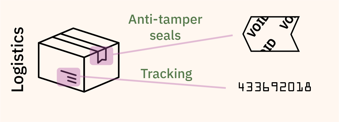
Unfortunately, the level of sophistication for verification at every level of the supply chain is precisely as much as it needs to be for the vendor to get away with it, and not one iota more. For example, when it comes to logistics, we largely rely upon anti-tamper seals and tracking numbers to make sure our package arrives intact.
These measures are generally effective at deterring petty theft, but most anti-tamper tape can be purchased by the roll on gray markets, and tracking updates are too infrequent to rule out package diversion and intervention. Besides, that, consumers are conditioned to accept packages that have been mis-routed or experienced an “exception” during delivery – few will return an item that was delivered a day late under fears that the item could have spent a night in a facility where back doors were installed. Our ready acceptance of delivery exceptions is just one example of how supply chains are only as tight as they need to be for broad consumer acceptance, and not one iota more.
Once you’ve received the shipping box, most high-end consumer electronics have additional seals on their packaging. Unfortunately, most seals rely on easy-to-copy anti-tamper solutions such as holograms or fine printing; or at best contain serial numbers that are easy to copy yet have no easy way to check for authenticity.
Solutions such as glitter seals or other stochastic seals that rely upon the randomness inherent in paper fiber or glue to create a unique, unforgeable seal for every package have been proposed, but adoption is low and there is a lack of standardized, easy-to-use verification tools for such seals. Again, packaging seals are just as good as they need to be for broad consumer acceptance, no more, no less.
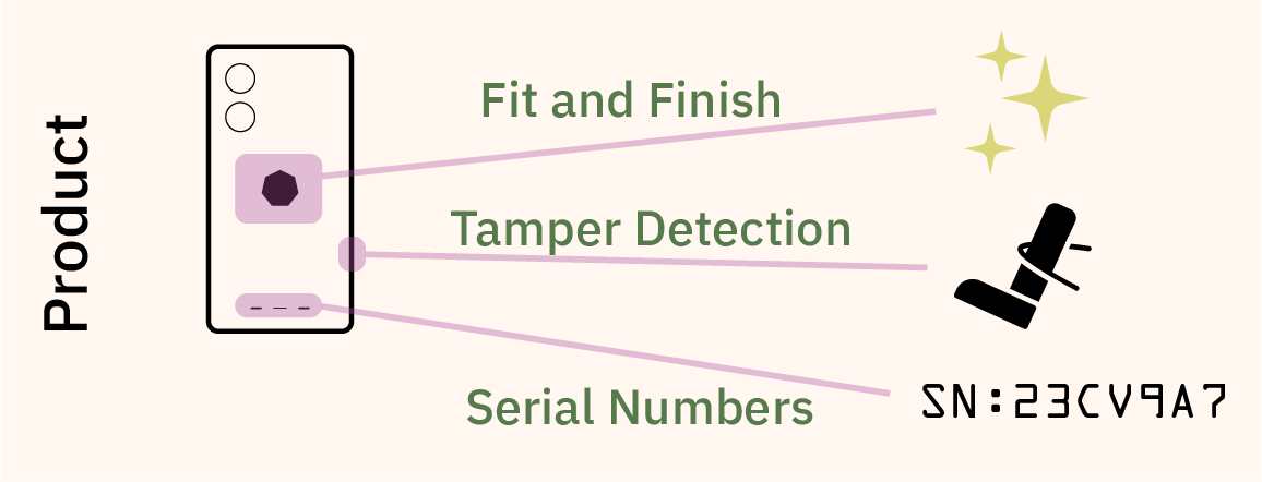
At the product level, there is a modicum of good news, at least in certain classes of products.
The traditional route of verification – observing the “fit and finish” of a product to detect counterfeits – is still the dominant method for most consumer products. However, in mobile phones and some laptops, manufacturers deploy electronic serial numbers and tamper detection techniques to deter would-be thieves of components or sub-assemblies. The effectiveness of these techniques depend intimately upon the implementation details; but in any case, they incur a cost in repairability and often times the end consumer can’t access the vendor’s databases to check that everything is in order. Instead, consumers are forced to delegate their trust to the vendors; yet regular consumers have no way to audit the vendors. The deferred trust boogeyman haunts everything from Apple’s iPhone ecosystem, to Intel’s SGX remote attestation mechanisms.
One would hope that this increase in verification sophistication is a trend that improves the deeper you go into the underlying technology. Unfortunately, it’s quite the opposite.
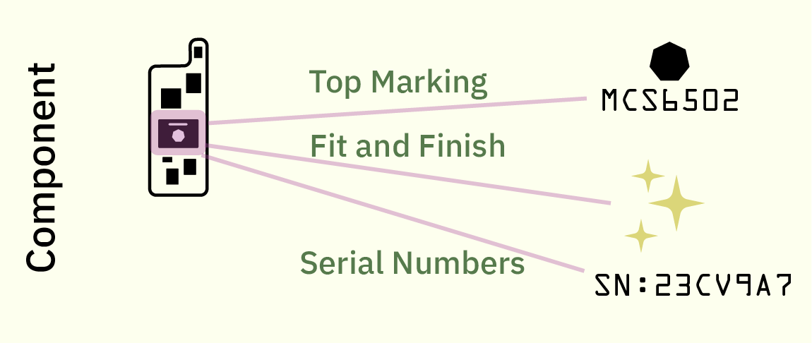
At the component level, the standard to this day for verifying the authenticity of a component is to look at the top marking (that is, the laser-etched numbers and logo) and the fit and finish of the package. Counterfeiters will often miss subtle details such as the font of the numbering, the location of the pin 1 marking, the composition of the overmold material, etc. Factories train staff to inspect and detect defects based on these irregularities.
What happens when a counterfeiter gets all these factors right? Well … the component goes into production, and we find out later about problems, either due to the assemblies failing test in the factory, or perhaps failing in peculiar ways in the field. For better or for worse, these problems are rare, generally affecting less than single-digit percentages of end users, and absent specific requirements or payments from customers to do more, equipment makers do exactly this and nothing more to protect the supply chain.
Even though most modern microcontrollers ship with an electronic serial number, few device manufacturers take advantage of them, and, perhaps somewhat surprisingly, there is usually no easy way to authenticate serial numbers with the component maker. Often times the purpose of the serial number is to serve as a unique ID for tracking products once manufactured; they are not structured to serve as a cryptographic method for determining provenance of the chip itself. Some security-forward microcontrollers feature things like PUFs (physically unclonable functions), but their implementation is usually directed at preventing people from tampering with or servicing their devices, rather than enabling users to verify the construction of the device itself.
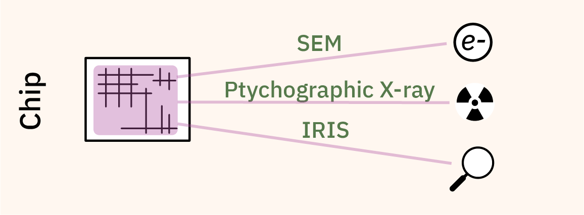
And that’s about it – this is where any attempt to verify our electronics stops. To a first order, nobody even looks at the wires inside the chip.
This is because prior to IRIS, your options for inspecting silicon are either destructive, or experiments conducted in high energy physics labs. If you’ve ever seen the brilliant teardowns done by companies like TechInsights, the chips are generally imaged at the circuit level with a SEM or FIB, which requires the chip to be removed from its package and some of the metal layers to be permanently stripped off. Thus, one can obtain extremely high-quality imagery of a sample chip, but these techniques cannot be used to verify the very chip you want to use inside your computer, as the imaged chip must be destroyed.
An alternative, non-destructive technique known as X-ray ptychography can be thought of as a very high resolution 3D scanner for circuits. It’s very impressive, but to date it can only be done in a handful of high energy physics labs and it takes a long time (about three hours for 20 cubic microns) to image a full chip.
The technique I’m developing, IRIS, is a non-destructive technique to acquire micron-resolution images of the first metal layer of a chip at a rate of a seconds per square millimeter. To the best of my knowledge, this is the first practical technique that gives users a glimpse of the actual circuits they will use after it has been mounted on a circuit board.
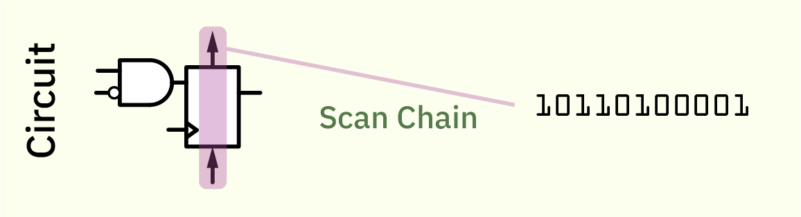
There’s one final layer deeper into the technology stack beyond imaging of the circuits: electrically testing the circuits directly with a technique known as a “scan chain”. The good news is that scan chains are a mature technology; the bad news is that it is almost never done by users because the details of the scan chain are kept secret, and that a scan chain inspection alone can be easily defeated by a malicious adversary.
The purpose of a scan chain is to assist with the rapid detection of fabrication defects. It works by adding an extra path to a finished design that strings every register into one or more chains. Bit patterns are loaded into the chain, and the resulting logical operations performed by the gates connected between the registers is observed on the output of the chain. With enough patterns, you can build up an idea of what logic is between every register. Of course, the space of bits to explore grows exponentially with the number of bits in a chain, so it’s not practical to brute-force a large state space.
As a result, scan chains are good for detecting flaws in known circuits introduced by mother nature, but ineffective at deterring a malicious adversary. This is true even if one could brute-force the entire state-space due to the epistemic circularity of trusting a circuit to test itself. More colloquially, one may have heard of the “Hawthorne Effect” or the “observer effect”, which describes a subject under study temporarily altering their behavior because they know they are being studied, thus affecting the results of the study. In this case, a scan chain knows when it’s being queried, and thus, a malicious modification to a scan chain can add hidden states that alter its behavior for the duration of a scan, allowing it to pretend to be correctly constructed, but only when a check is actively running.
Although almost every chip goes through a scan chain test before it is shipped, the test vectors are proprietary, and often times the scan chains are deliberately and permanently sealed in a way to make it impossible for users to access. Scan chains may be scuttled after the factory test for ostensible security reasons, as an adversary can use them to read out the full state of a chip. However, depending on the threat model, it may be preferable to give users the option to exercise the scan chain and then permanently fuse out the scan chain after inspection.
Filling in the Verification Gap
As the summary chart below shows, supply chain verification techniques, although imperfect, enjoy broad adoption at the component level and above. However, there is a significant gap in user verification starting at the chip level and below.
My work, the Infra-Red, in situ (IRIS) inspection of silicon, is a step toward filling in this verification gap. In its simplest form, chips are deliberately constructed for optical inspection with infra-red light shined through the back side of the chip – that is, the side facing “up” that is not bonded to the circuit board.
The technique works because although silicon looks opaque at visible light, it is transparent starting at near-infrared wavelengths (roughly 1000 nm and longer). Today’s commodity optics and CMOS cameras are actually capable of working with lights at this wavelength; thus, IRIS is a low-cost and effective technique for confirming the construction of chips down to block level. For example, IRIS can readily help determine if a chip has the correct amount of RAM, number of CPU cores, peripherals, bond pads, etc. This level of verification would be sufficient to deter most counterfeits or substitutions.
However, due to the diffraction limit of infra-red light, it is insufficient for transistor-level imaging. Furthermore, it can only reliably infer the existence of the metal layers closest to the transistors (in technical jargon, it can infer the existence of “standard cell” library elements); it cannot reveal too much information about the higher-level metal wires that route between logic gates.
Thus, for threat models which require protection against adversaries capable of manipulating wires on an integrated circuit, IRIS should be combined with scan chain techniques to robustly verify a chip’s construction.
Hybrid Verification For the Win
As alluded to previously, scan chains alone are insufficient for detecting modifications to a circuit, because an adversary may modify the scan chain in such a manner that it responds with correct answers during the scan itself, but behaves maliciously otherwise.
However, such modifications require the introduction of additional logic gates to track the scan state and compute both correct and malicious responses. Because IRIS can “see” logic gates, it is able to put a firm upper bound on the potential amount of additional logic present in an integrated circuit. Thus, the combination of IRIS and scan chain techniques may be able to effectively verify that a circuit is correctly constructed.
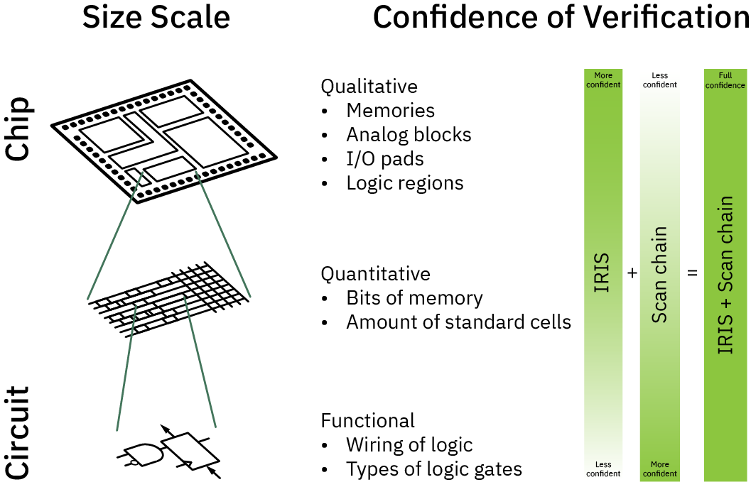
The diagram above illustrates how IRIS and scan chain techniques compliment each other to obtain a high-confidence verification of a chip’s structure.
At the largest scales, IRIS can trivially quantify the number of IP blocks, pads, analog functions and memories; this is in contrast to scan-chain techniques which may struggle to characterize analog functions and other macro-scale properties, due to factors such as the analog limitations of scan chains, and the exponential growth of state-space to explore at the macro-level.
At intermediate scales, IRIS can quantify the number of bits of memory, or bound the number of standard cells in a region. This places constraints on how much malicious logic could be injected that could otherwise defeat a scan chain test.
At the smallest scales, IRIS cannot discern individual wires or gates. However, scan chain excels at exploring the topology and function of logic at the smallest and most local increments.
Thus, in combination, the two techniques may be used to achieve a high confidence verification of a chip’s function – at a cost and time scale suitable for point-of-use (e.g. end user) verification. I say “high confidence” because in the end, there is a probabilistic nature to both imaging and scan chain pattern coverage. As future work I’d like to explore the possibility of using formal methods to mathematically rule out any escapes, but absent formal proofs, it is important to understand that the technique is probabilistic in nature. That being said, it is still vastly better than the current state of the art, which is doing nothing at all.
Hybrid verification could be a viable path toward filling in the verification gap at the most fundamental levels of the supply chain, assuming chip vendors are willing to facilitate such verification by designing and packaging their products in a manner conducive to optical verification, and assuming chip vendors are willing to share scan chain test vectors with end users.
IRIS: Where We Are, and Where We are Headed
Because of the 1000 nm wavelength limit imposed by the transparency of silicon, IRIS has a limit on the features it can resolve. Below is an example IRIS imaging a small part of a RISC-V core on a 130nm chip fabricated using the SKY130A open PDK from Matt Venn’s MPW7 run; you can browse the entire chip image here.
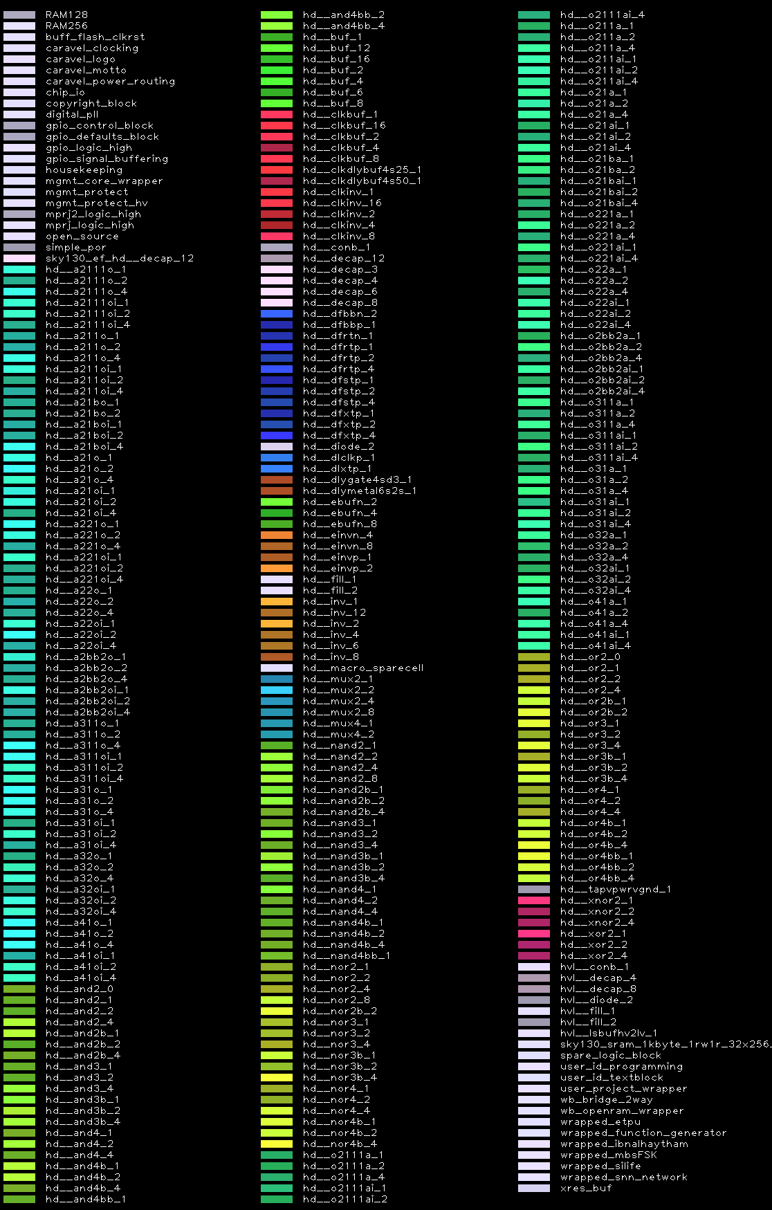
Use the slider to compare the base image against an overlay derived from the design files. Each colored rectangle in the overlay corresponds to a “standard cell”: blue are flip flops, pink are filler/capacitor cells, aqua are varieties of and-or-invert gates, etc. Note that the native resolution of the image above is 1469 pixels wide; it has been scaled down to fit the width of this page.
One can see that in a 130nm process, IRIS has a reasonable chance of conducting a gate-count census of an entire chip. And yes, it’s not atypical for chips to be limited not by logic density, but by wiring density; hence, the majority of a chip’s active area contains filler cells (the pink rectangles).
Above is of an identically scaled region of a 22nm chip, again of a RISC-V core, but this time almost the entire core is within view because the logic gates are, unsurprisingly, much smaller: a single gate can be as small as a few pixels. At this node, IRIS can place an upper bound on gate count to within a couple dozen extra flip flops.
An important caveat when comparing images above: the backside finish of the 130nm chip is a mirror polish, but the 22nm chip only went through backgrinding; in other words, the 22nm chip’s image clarity is degraded due to a series of small surface ridges that refract light. If the 22nm chip had the same mirror-finish quality as the 130nm chip, the imaging resolution of the 22nm chip would be improved. Back side polishing of chips is not a difficult or uncommon process, but it’s not done unless explicitly required. Thus, chips intended for optical verification should specify a high quality mirror finish for the back side.
IRIS goes hand-in-hand with electrical scan chains to achieve full chip verification. Scan chains are able to quickly confirm the wiring between small clusters of standard cells, but Trojans can evade detection by including an honest copy of the affected logic. IRIS confirms that a given cluster of logic being tested by a scan chain is approximately the right size. The search perimeter for rouge cells is reduced by running the scan chain test at high speeds. Ideally, the total bounds are tight enough to rule out the existence of sufficient extra logic to evade detection in scan chain testing.
In other words, what IRIS can’t directly image, the scan chain has to make up for with complexity of test. Thus, at 130nm, a simple bit-shift scan chain may be sufficient, since individual gates are resolvable; at 22nm, a more complicated technique splitting the scan chain into multiple segments, capable of challenging the system with mutually unpredictable data patterns, may be required to drive up the lower bound on circuit complexity to the “dozens of logic gates” range required to bypass the test. And at the most advanced nodes, even more scan chain segments may be required along with supplementary design techniques to drive the lower confidence bound into the “hundreds of logic gates” range for reliable Trojan detection with IRIS.
In general, when I use the term “IRIS” alone in a context where high-confidence gate level verification is required, readers should infer that I’m referring to some kind of hybrid verification technique of both IRIS and scan chain.
That being said, I envision IRIS mainly being used to verify high-value circuitry, such as those found in a discrete cryptographic enclave intended to store secrets such as root keys. These enclaves would not require the performance or density of the latest process nodes. With careful design, a 22nm or 28nm process can offer GHz clock speeds, sufficient for storing and processing bulk data with root secrets. The “2x” nm node is particularly interesting because it is the best “value per transistor” sweet-spot, and likely to stay that way for the foreseeable future: it’s the smallest process node that still uses the easier-to-fabricate planar CMOS transistors while requiring only single-patterning DUV lithography techniques.
Thus, the bulk of my on-going research will focus on samples produced in 130nm and 180nm (because there are Open PDKs available for those nodes today), and 22nm (because of the ultimate economic importance of the node). I am also betting that while the 2x nm node is not open source today, it will become more open within the next decade if the world continues on a “business as usual” scenario where technology continues to race down the commodification curve, and fabs continue to compete on price and need more designs to keep them busy and profitable.
While the imaging system has met its initial goals, the software still has miles to go before I sleep (And miles to go before I sleep). In particular, I’m still working on training a computer to automatically recognize patterns of gates in IRIS images and to generate a gate count census. I’d also ideally like to find a way to use formal methods to place an upper bound on the amount of logic one can hide in a scan chain for a given testing methodology, so designers can have a formally proven tool to validate that their scan chains are sufficiently dense so that IRIS can pick up any attempts to bypass them. Unfortunately, I’m neither a software engineer nor a mathematician, but the problems are interesting enough that I’ll still give them a go. Worst case, I will learn something new along the path to failure.
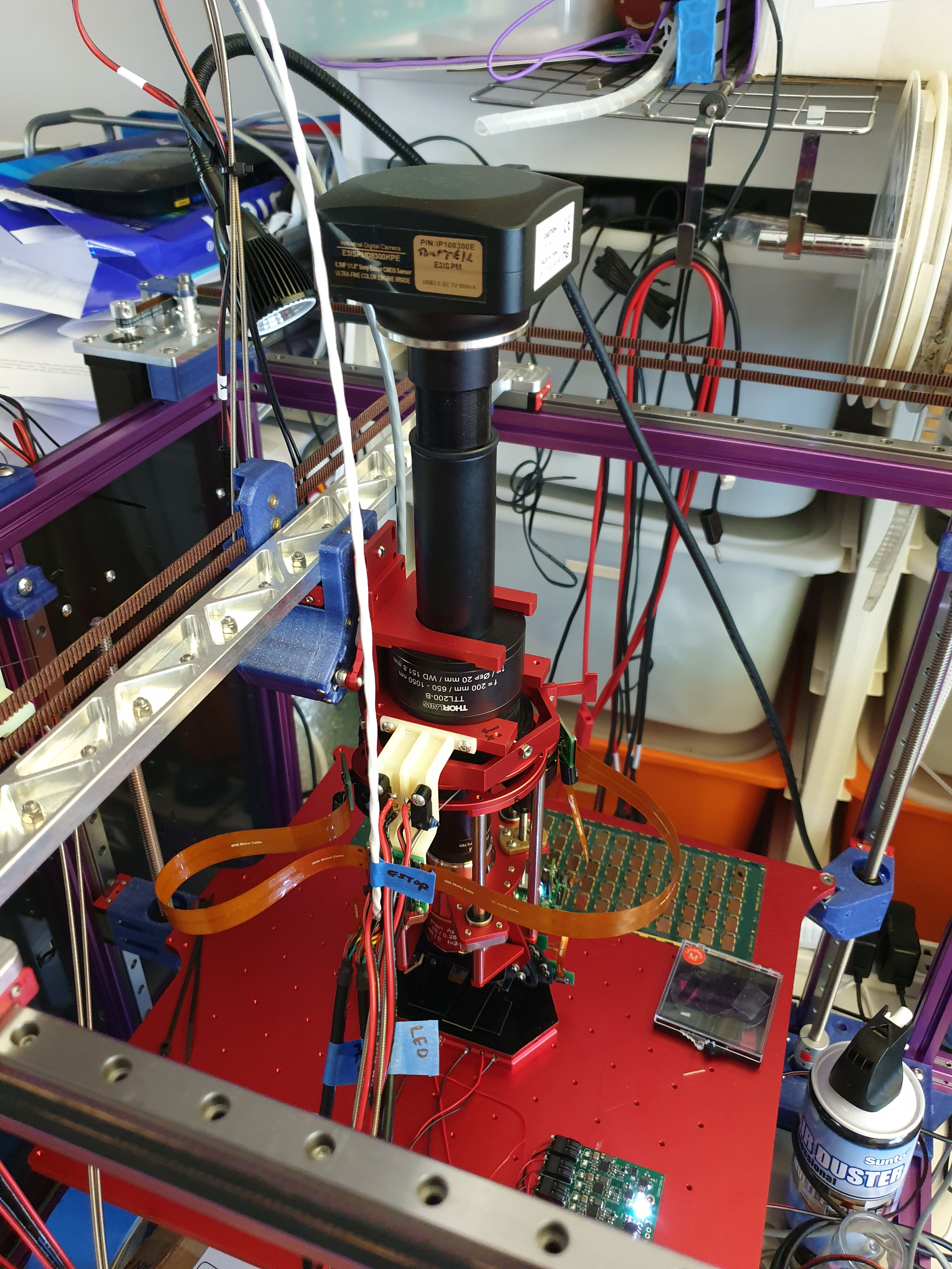
Above is the IRIS machine that I’ve built. There’s a lot going on here – but basically, it’s an IR camera attached to a microscope, a nanometer-resolution focusing mechanism, and a pair of 1050nm light sources that have continuously adjustable azimuth and zenith. This microscope assembly is mounted in a Jubilee motion platform. The Jubilee is open source, and was designed by Sonya Vasquez of Prof. Nadya Peek‘s Machine Agency group. I got it as a kit from Filastruder. The base motion platform is capable of 10 micron steps, and features a kinematically coupled Z-bed with three independent actuators, allowing me to dynamically compensate for planarity issues in the sample undergoing imaging.
Above is a short video loop showing the core mechanics in action. The weird thing on the bottom with the red and black wires coming out of it is the kinematically coupled nanometer-resolution fine focus stage; its motions are too small to be picked up by the camera.
An explicit goal of this project is to open source all of IRIS, so that anyone can replicate the imaging system. Democratizing chip verification is important because a credible threat of being caught reduces the incentive of adversaries to deploy expensive Trojan-implantation capabilities.
With little fear of being caught, there’s a payoff even if an adversary has to plow tens of millions of dollars into a capability for planting chip-level hardware Trojans in high-value targets. However, if chip inspection equipment can purchased in the ballpark of hundreds to perhaps thousands of dollars, and more than a handful of users are known to routinely inspect chips, the path to payoff for an adversary before they are caught becomes murky. In this case, a rational adversary may be deterred from targeting an IRIS-enabled design, instead reserving their capabilities only for the chips that are difficult to inspect.
Aside from that, I’ll be straight with you – a big motivation for IRIS is simply because I am curious, and I want to look inside chips and see how they are built (and it’s kind of fun and strangely satisfying to build robots). I haven’t been disappointed with what I’ve seen so far – I have to stop myself from wasting evenings browsing through the construction of chips. I’ve done a bit of chip design in the past, and it’s fascinating to see the diversity of techniques and new trends in chip designs. I’m excited to share this sense of wonder with kindred spirits!
Given the volume of material to cover, I’m going to break the documentation up into a series of blog posts that go into the methodology used to build the machine, as well as details about every custom component, and the design decisions that went into them. I’ll also summarize the status of the analysis software that accompanies the system – so stay tuned for more posts!
Finally, a big shout-out to NLnet and the European Commission. NLnet’s NGI0 Entrust fund, established with support from the European Commission’sNext Generation Internet Program, are instrumental in facilitating my work on IRIS. Also a big shout-out to my Github Sponsors for their incredible generosity and monthly support. Thanks to all these donors, I’m able to keep IRIS 100% open source and free of conflicts of interest with commercial investors.
Cryptography tells us how to make a chain of trust rooted in special-purpose chips known as secure elements. But how do we come to trust our secure elements? I have been searching for solutions to this thorny supply chain problem. Ideally, one can directly inspect the construction of a chip, but any viable inspection method must verify the construction of silicon chips after they have been integrated into finished products, without having to unmount or destroy the chips (“in situ“). The method should also ideally be cheap and simple enough for end users to access.
This post introduces a technique I call “Infra-Red, In Situ” (IRIS) inspection. It is founded on two insights: first, that silicon is transparent to infra-red light; second, that a digital camera can be modified to “see” in infra-red, thus effectively “seeing through” silicon chips. We can use these insights to inspect an increasingly popular family of chip packages known as Wafer Level Chip Scale Packages (WLCSPs) by shining infrared light through the back side of the package and detecting reflections from the lowest layers of metal using a digital camera. This technique works even after the chip has been assembled into a finished product. However, the resolution of the imaging method is limited to micron-scale features.
This post will start by briefly reviewing why silicon inspection is important, as well as some current methods for inspecting silicon. Then, I will go into the IRIS inspection method, giving background on the theory of operation while disclosing methods and initial results. Finally, I’ll contextualize the technique and discuss methods for closing the gap between micron-scale feature inspection and the nanometer-scale features found in today’s chip fabrication technology.
Many assume the point of trustable hardware is so that a third party can control what you do with your computer – like the secure enclave in an iPhone or a TPM in a PC. In this model, users delegate trust to vendors, and vendors do not trust users with key material: anti-tamper measures take priority over inspectability.
Readers who make this assumption would be confused by a trust method that involves open source and user inspections. To be clear, the threat model in this post assumes no third parties can be trusted, especially not the vendors. The IRIS method is for users who want to be empowered to manage their own key material. I acknowledge this is an increasingly minority position.
Why Inspect Chips?
The problem boils down to chips being literal black boxes with nothing but the label on the outside to identify them.
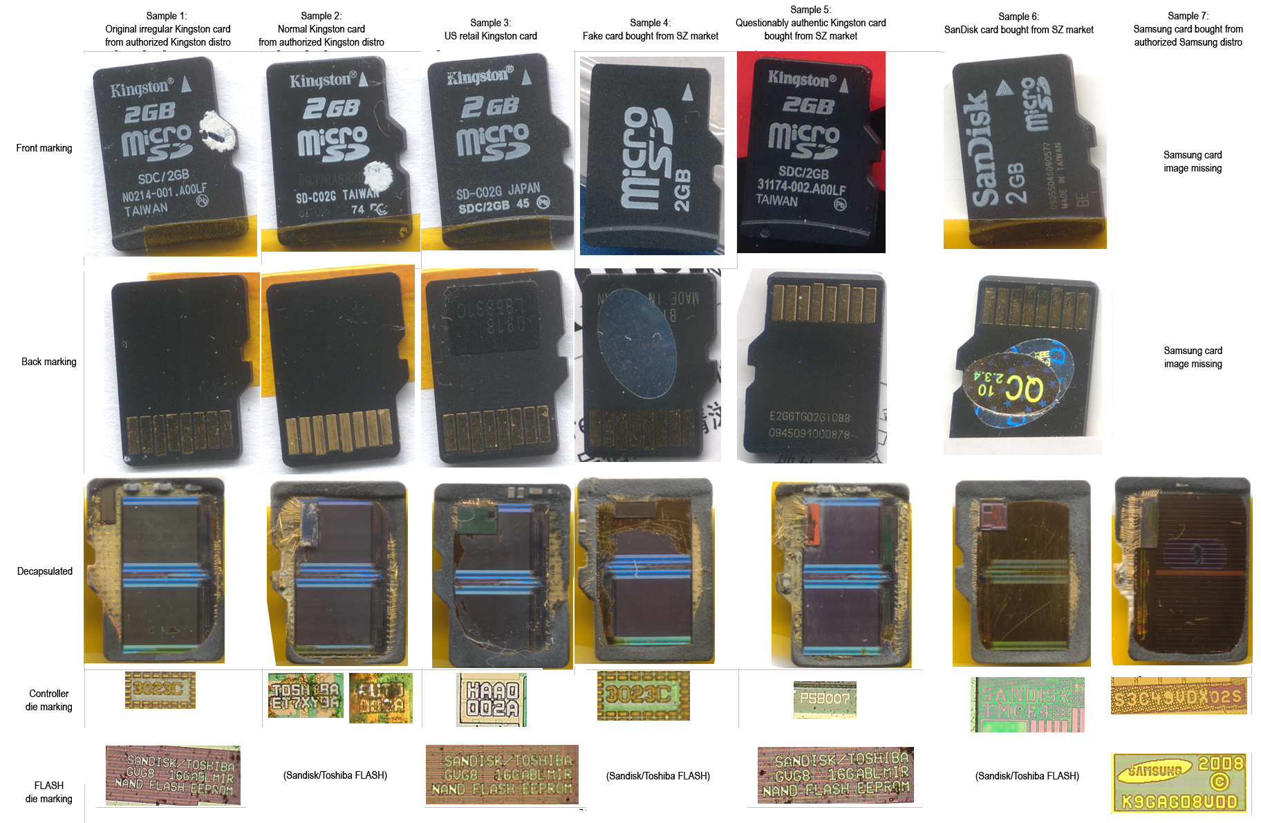
For example, above is a study I performed surveying the construction of microSD cards in an effort to trace down the root cause of a failed lot of products. Although every microSD card ostensibly advertised the same product and brand (Kingston 2GB), a decap study (where the exterior black epoxy is dissolved using a strong acid revealing the internal chips while destroying the card) revealed a great diversity in internal construction and suspected ghost runs. The take-away is that labels can’t be trusted; if you have a high-trust situation, something more is needed to establish a device’s internal construction than the exterior markings on a chip’s package.
What Are Some Existing Options for Inspecting Chips?
There are many options for inspecting the construction of chips; however, all of them suffer from a “Time Of Check versus Time Of Use” (TOCTOU) problem. In other words, none of these techniques are in situ. They must be performed either on samples of chips that are merely representative of the exact device in your possession, or they must be done at remote facilities such that the sample passes through many stranger’s hands before returning to your possession.
Scanning Electron Microscopy (SEM), exemplified above, is a popular method for inspecting chips (image credit: tmbinc). The technique can produce highly detailed images of even the latest nanometer-scale transistors. However, the technique is destructive: it can only probe the surface of a material. In order to image transistors one has to remove (through etching or polishing) the overlying layers of metal. Thus, the technique is not suitable for in situ inspection.
X-rays, exemplified in the above image of a MTK6260DA , are capable of non-destructive in situ inspection; anyone who has traveled by air is familiar with the applicability of X-rays to detect foreign objects inside locked suitcases. However, silicon is nearly transparent to the types of X-rays used in security checkpoints, making it less suitable for establishing the contents of a chip package. It can identify the size of a die and the position of bond wires, but it can’t establish much about the pattern of transistors on a die.
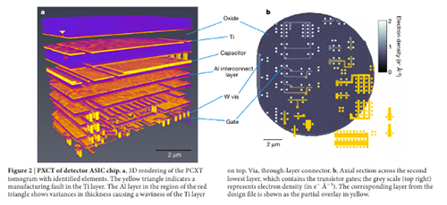
X-Ray Ptychography is a technique using high energy X-rays that can non-destructively establish the pattern of transistors on a chip. The image above is an example of a high-resolution 3D image generated by the technique, as disclosed in this Nature paper.
It is a very powerful technique, but unfortunately it requires a light source the size of a building, such as the Swiss Light Source (SLS) (donut-shaped building in the image above), of which there are few in the world. While it is a powerful method, it is impractical for inspecting every end user device. It also suffers from the TOCTOU problem in that your sample has to be mailed to the SLS and then mailed back to you. So, unless you hand-carried the sample to and from the SLS, your device is now additionally subject to “evil courier” attacks.
Optical microscopy – with a simple benchtop microscope, similar to those found in grade-school classrooms around the world – is also a noteworthy tool for inspecting chips that is easier to access than the SLS. Visible light can be a useful tool for checking the construction of a chip, if the chip itself has not been obscured with an opaque, over-molded plastic shell.
Fortunately, in the world of chip packaging, it has become increasingly popular to package chips with no overmolded plastic. The downside of exposing delicate silicon chips to possible mechanical abuse is offset by improved thermal performance, better electrical characteristics, smaller footprints, as well as typically lower costs when compared to overmolding. Because of its compelling advantages this style of packaging is ubiquitous in mobile devices. A common form of this package is known as the “Wafer Level Chip Scale Package” (WLCSP), and it can be optically inspected prior to assembly.
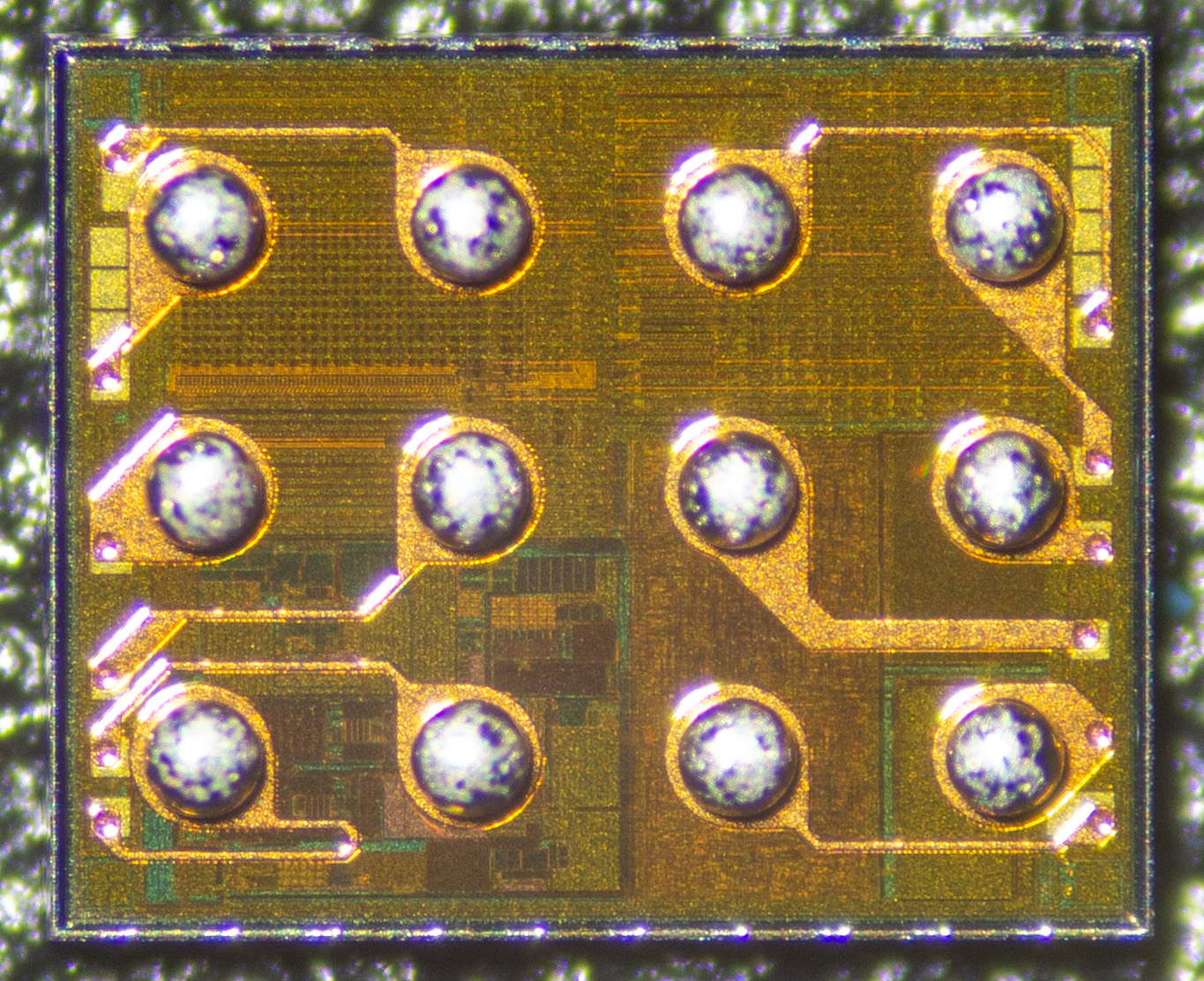
Above is an example of such a package viewed with an optical microscope, prior to attachment to a circuit board. In this image, the back side of the wafer is facing away from us, and the front side is dotted with 12 large silvery circles that are solder balls. The spacing of these solder balls is just 0.5mm – this chip would easily fit on your pinky nail.
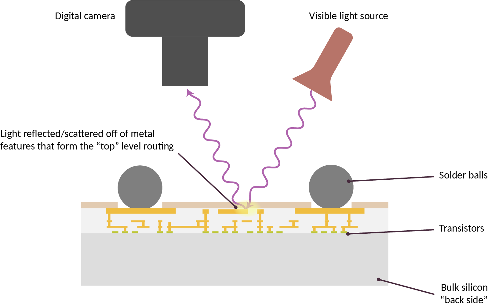
The imaged chip is laying on its back, with the camera and light source reflecting light off of the top level routing features of the chip, as illustrated in the cross-section diagram above. Oftentimes these top level metal features take the form of a regular waffle-like grid. This grid of metal distributes power for the underlying logic, obscuring it from direct optical inspection.
Note that the terms “front” and “back” are taken from the perspective of the chip’s designer; thus, once the solder balls are attached to the circuit board, the “front side” with all the circuitry is obscured, and the plain silvery or sometimes paint-coated “back side” is what’s visible.
As a result, these chip packages look like opaque silvery squares, as demonstrated in the image above. Therefore front-side optical microscopy is not suitable for in situ inspection, as the chip must be removed from the board in order to see the interesting bits on the front side of the chip.
The IRIS Inspection Method
The Infra-Red, In Situ (IRIS) inspection method is capable of seeing through a chip already attached to a circuit board, and non-destructively imaging the construction of a chip’s logic.
Here’s a GIF that shows what it means in practice:
We start with an image of a WLCSP chip in visible light, assembled to a finished PCB (in this case, an iPhone motherboard). The scene is then flooded with 1070 nm infrared light, causing it to take on a purplish hue. I then turn off the visible light, leaving only the infrared light on. The internal structure of the chip comes into focus as we adjust the lens. Finally, the IR illuminator is moved around to show how the chip’s internal metal layers glint with light reflected through the body of the silicon.
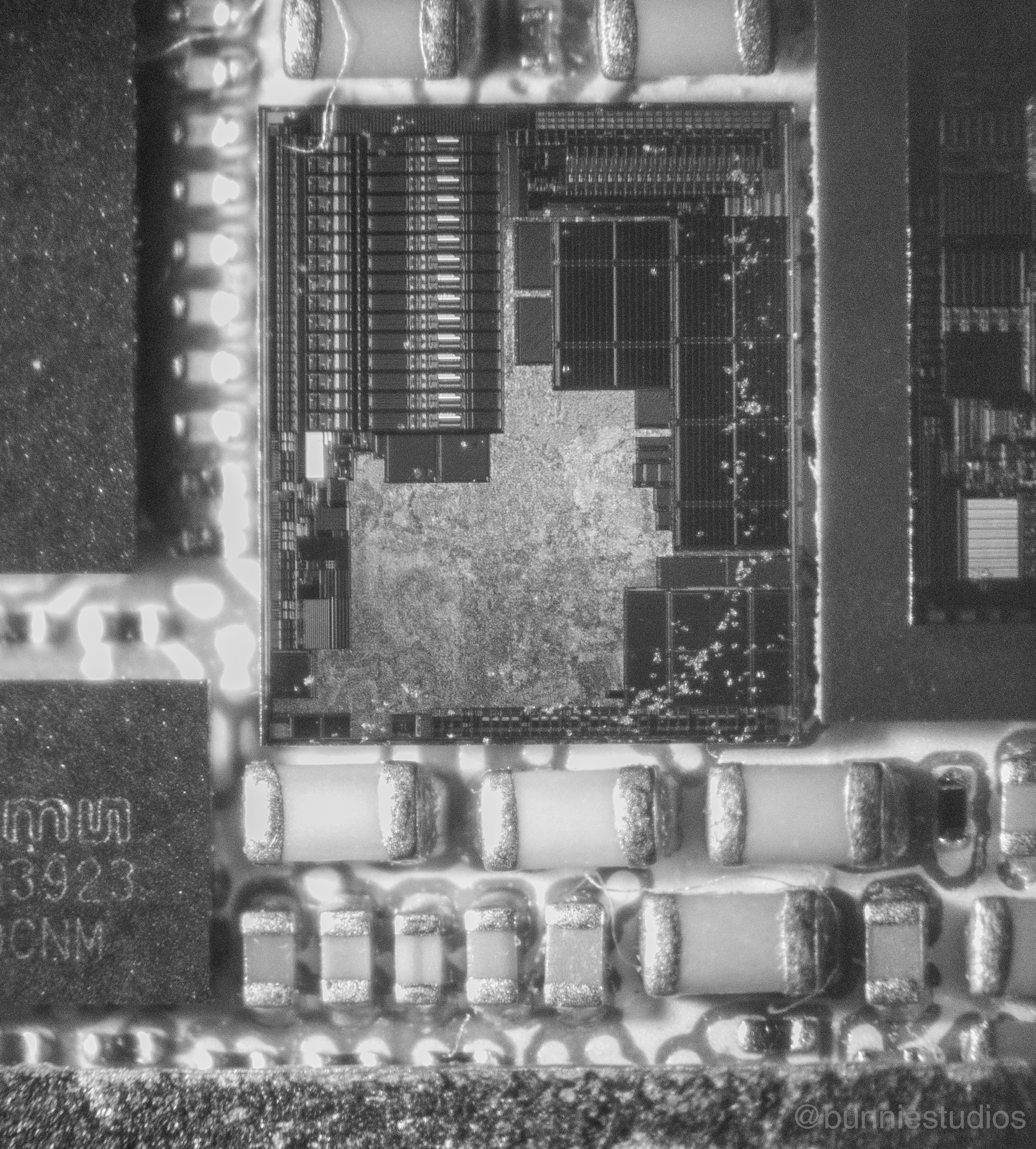
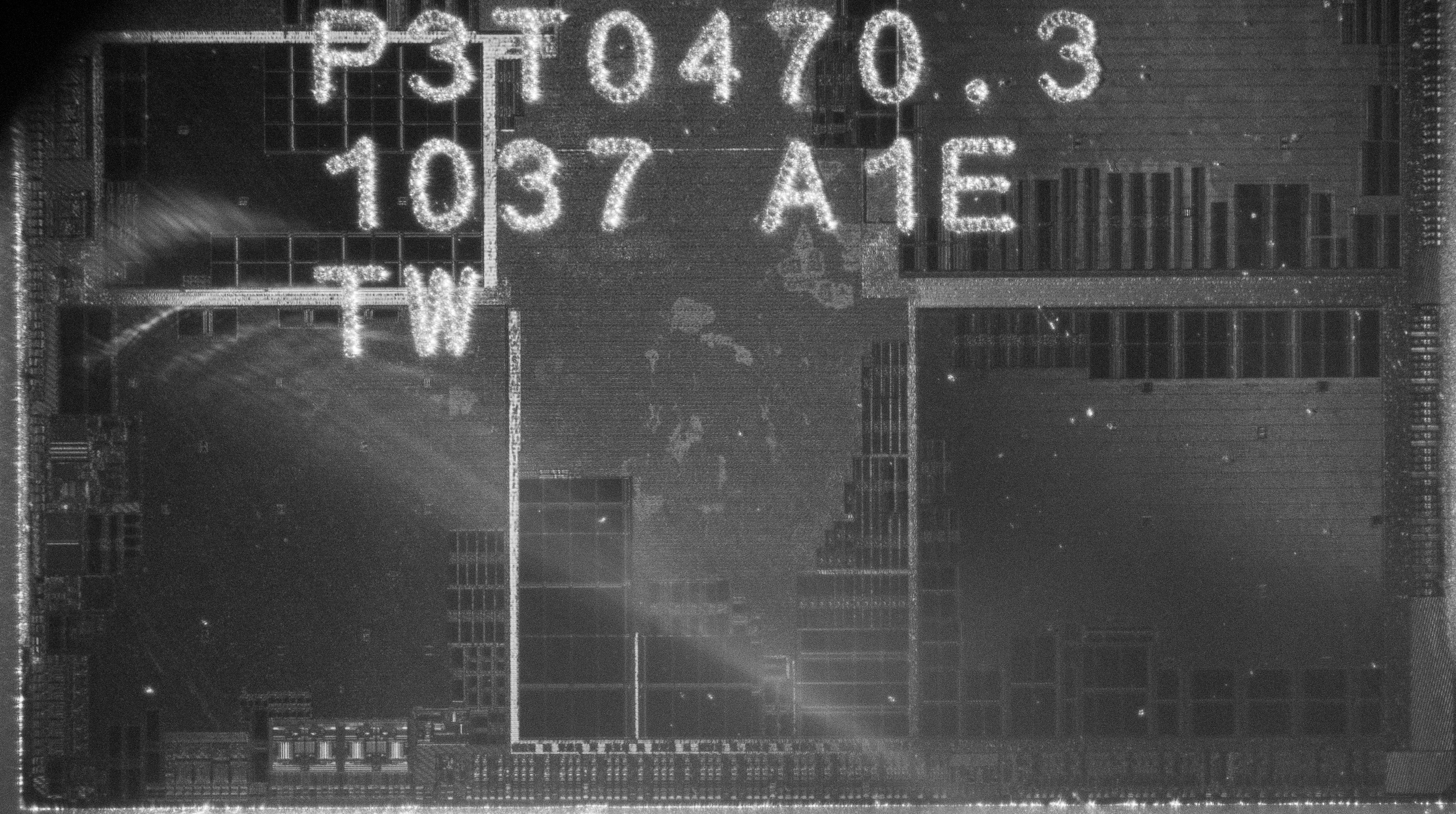
Here is a still image of the above chip imaged in infra-red, at a higher resolution:
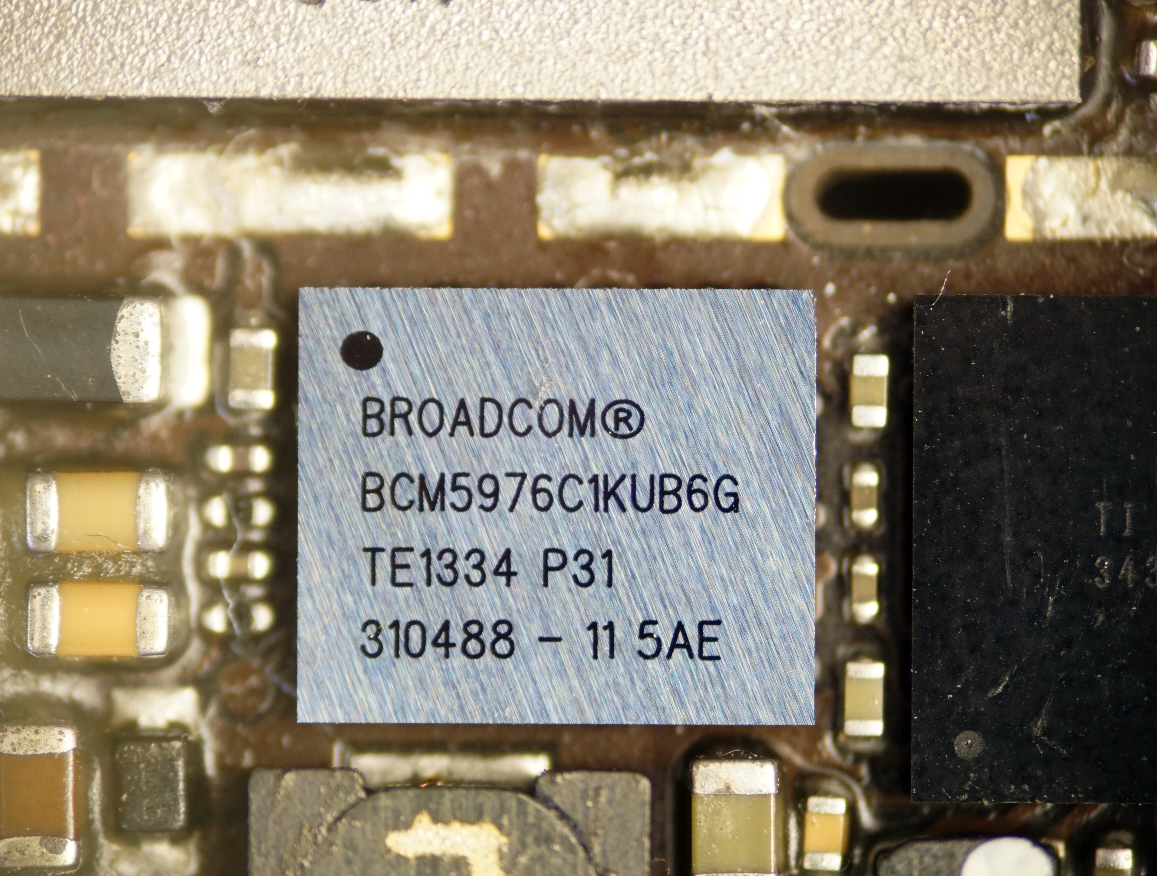
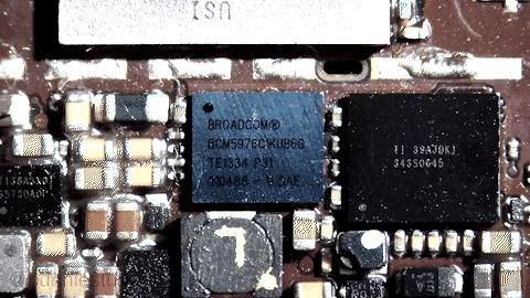
The chip is the BCM5976, a capacitive touchscreen driver for older models of iPhones. The image reveals the macro-scopic structure of the chip, with multiple channels of data converters on the top right and right edge, along with several arrays of non-volatile memory and RAM along the lower half. From the top left extending to the center is a sea of standard cell logic, which has a “texture” based on the routing density of the metal layers. Remember, we’re looking through the backside of the chip, so the metal layer we’re seeing is mostly M1 (the metal connecting directly to the transistors). The diagonal artifacts apparent through the standard cell region are due to a slight surface texture left over from wafer processing.
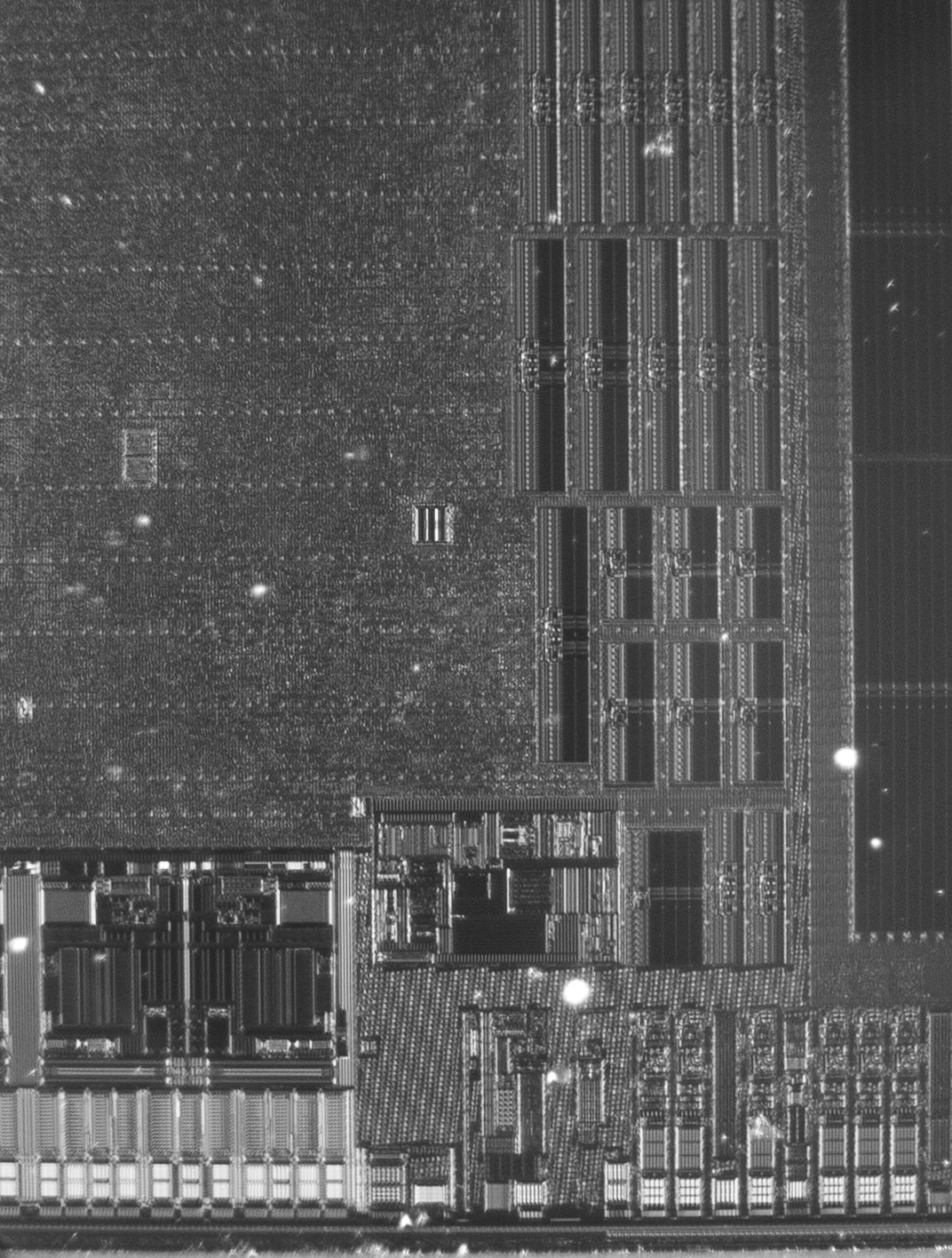
Below is the region in the pink rectangle at a higher magnification (click on the image to open a full-resolution version):
The magnified region demonstrates the imaging of meso-scopic structures, such as the row and structure column of memory macros and details of the data converters.
The larger image is 2330 pixels wide, while the chip is 3.9 mm wide: so each pixel corresponds to about 1.67 micron. To put that in perspective, if the chip were fabricated in 28 nm that would correspond to a “9-track” standard cell logic gate being 0.8 microns tall (based on data from Wikichip). Thus while these images cannot precisely resolve individual logic gates, the overall brightness of a region will bear a correlation to the type and density of logic gate used. Also please remember that IRIS is still at the “proof of concept” stage, and there are many things I’m working on to improve the image quality and fidelity.
Here’s another demo of the technique in action, on a different iPhone motherboard:
How Does It Work?
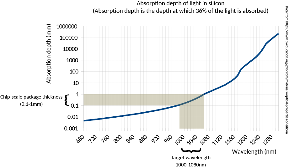
Silicon goes from opaque to transparent in the range of 1000 nm to 1100 nm (shaded band in the illustration below). Above 1100 nm, it’s as transparent as a pane of glass; below 1000 nm, it rapidly becomes more opaque than the darkest sunglasses.
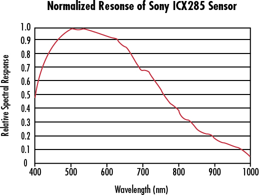
Meanwhile, silicon-based image sensors retain some sensitivity in the near-to-short wave IR bands, as illustrated below.
Between these two curves, there is a “sweet spot” where standard CMOS sensors retain some sensitivity to short-wave infrared, yet silicon is transparent enough that sufficient light passes through the layer of bulk silicon that forms the back side of a WLCSP package to do reflected-light imaging. More concretely, at 1000 nm a CMOS sensor might have 0.1x its peak sensitivity, and a 0.3 mm thick piece of silicon may pass about 10% of the incident light – so overall we are talking about a ~100x reduction in signal intensity compared to visible light operations. While this reduction is non-trivial, it is surmountable with a combination of a more intense light source and a longer exposure time (on the order of several seconds).
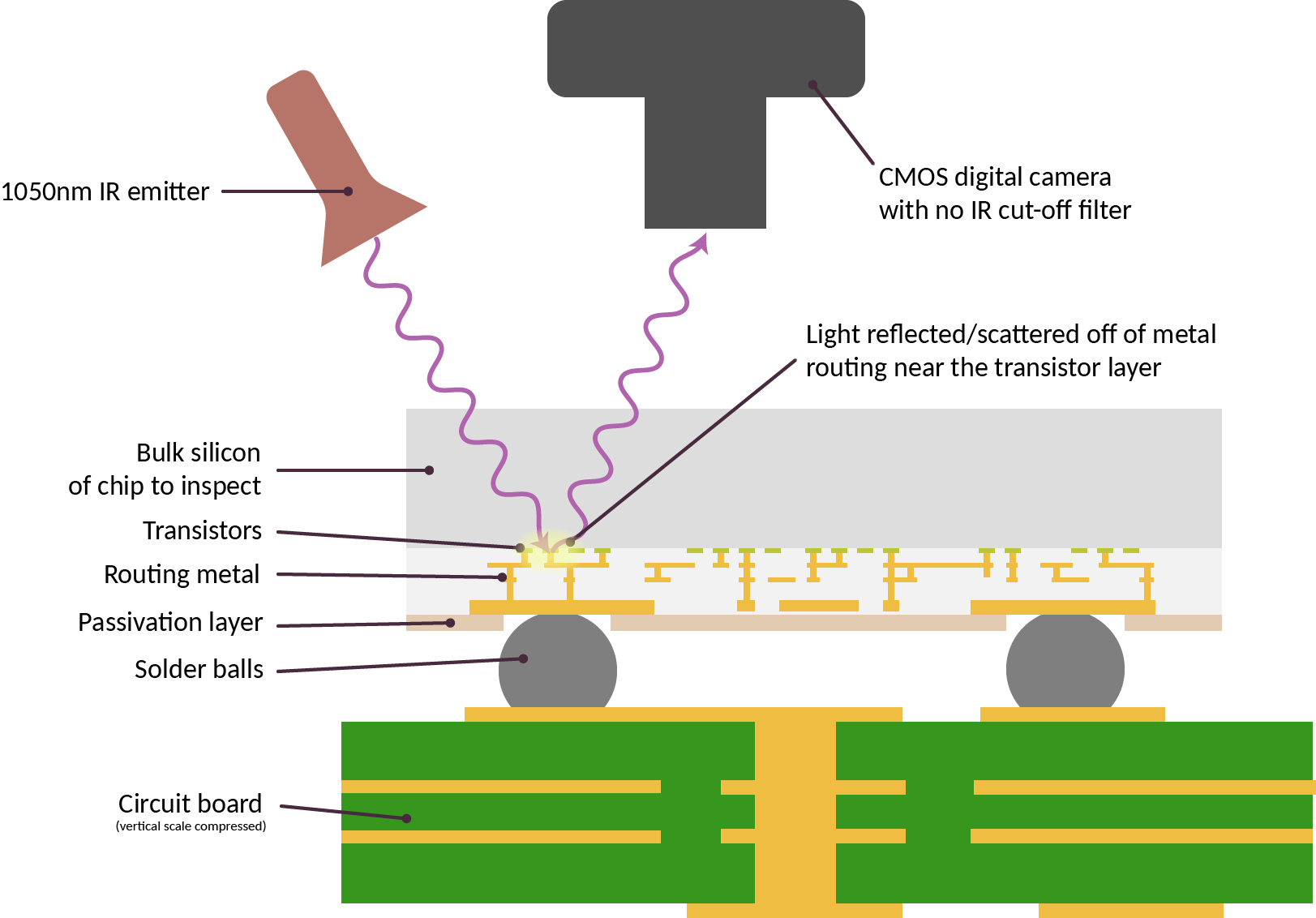
Above is a cross-section schematic of the IRIS inspection setup. Here, the sample for inspection is already attached to a circuit board and we are shining light through the back side of the silicon chip. The light reflects off of the layers of metal closest to the transistors, and is imaged using a camera. Conceptually, it is fairly straightforward once aware of the “sweet spot” in infrared.
Two things need to be prepared for the IRIS imaging technique. First, the “IR cut-off filter” has to be removed from a digital camera. Normally, the additional infrared sensitivity of CMOS sensors is considered to be problematic, as it introduces color fidelity artifacts. Because of this excess sensitivity, all consumer digital cameras ship with a special filter installed that blocks any incoming IR light. Removing this filter can range from trivial to very complicated, depending on the make of the camera.
Second, we need a source of IR light. Incandescent bulbs and natural sunlight contain plenty of IR light, but the current demonstration setup uses a pair of 1070 nm, 100 mA IF LED emitters from Martech, connected to a simple variable current power supply (in practice any LED around 1050nm +/- 30nm seems to work fairly well).
To give credit where it’s due, the spark for IRIS came from a series of papers referred to me by Dmitry Nedospadov during a chance meeting at CCC. One published example is “Key Extraction Using Thermal Laser Stimulation” by Lohrke et al, published in IACR Transactions on Cryptographic Hardware and Embedded Systems (DOI:10.13154/tches.v2018.i3.573-595). In this paper, a Phemos-1000 system by Hamamatsu (a roughly million dollar tool) uses a scanning laser to do optical backside imaging of an FPGA in a flip-chip package. More recently, I discovered a photo feed by Fritzchens Fritz demonstrating a similar technique, but using a much cheaper off-the-shelf Sony NEX-5T. Since then, I have been copying these ideas and improving upon them for practical application in supply chain/chip verification.
How Can I Try It Out?
While “off the shelf” solutions like the Phemos-1000 from Hamamatsu can produce high-resolution backside images of chips, the six or seven-figure price tag puts it out of reach of most practical applications. I have been researching ways to scale this cost down to something more accessible to end-users.
In the video below, I demonstrate how to modify an entry-level digital inspection camera, purchasable for about $180, to perform IRIS inspections. The modification is fairly straightforward and takes just a few minutes. The result is an inspection system that is capable of performing, at the very least, block-level verification of a chip’s construction.
For those interested in trying this out, this is the $180 camera and lens combo from Hayear (link contains affiliate code) used in the video. If you don’t already have a stand for mounting and focusing the camera, this one is pricey, but solid. You’ll also need some IR LEDs like this one to illuminate the sample. I have found that most LEDs with a 1050-1070 nm center wavelength works fairly well. Shorter wavelength LEDs are cheaper, but the incidentally reflected light off the chip’s outer surface tends to swamp the light reflected by internal metal layers; longer than 1100 nm, and the camera efficiency drops off too much and the image is too faint and noisy.
Of course, you can get higher quality images if you spend more money on better optics and a better camera. Most of the images shown in this post were taken with a Sony A6000 camera that was pre-modified by Kolari Vision. If you have a spare camera body laying around it is possible to DIY the IR cut-off filter removal; YouTube has several videos showing how.
The modified camera was matched with either the optics of the previously-linked Hayear inspection scope, or directly attached to a compound microscope via a C-mount to E-mount adapter.
Another Sample Image
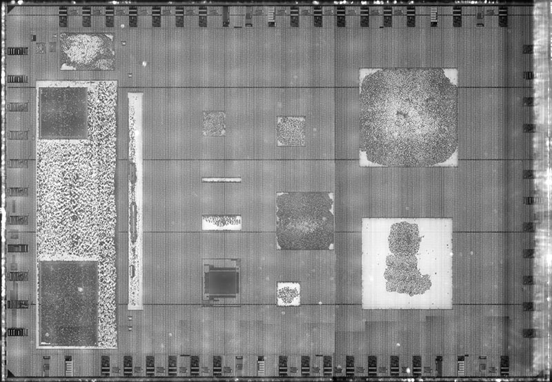
I’ve been using an old Armada610 chip I had laying around for testing the setup. It’s ideal for testing because I know the node it was fabbed in (55 nm) and the package is a bare flip-chip BGA. FCBGA is a reasonably common package type, but more importantly for IRIS, the silicon is pre-thinned and mirror-polished. This is done to improve thermal performance, but it also makes for very clean backside images.
Above is what the chip looks like in visible light.
And here’s the same chip, except in IR. The light source is shining from the top right, and already you can see some of the detail within the chip. Note: the die is 8mm wide.
Above is the lower part of the chip, taken at a higher magnification. Here we can start to clearly make out the shapes of memory macros, I/O drivers, and regions of differing routing density in the standard cell logic. The die is about 4290 pixels across in this image, or about 1.86 microns per pixel.
And finally, above is the boxed region in the previous image, but a higher magnification (you can click on any of the images for a full-resolution version). Here we can make out the individual transistors used in I/O pads, sense amps on the RAM macros, and the texture of the standard cell logic. The resolution of this photo is roughly 1.13 microns per pixel – around the limit of what could be resolved with the 1070 nm light source – and a hypothetical “9-track” standard cell logic gate might be a little over a pixel tall by a couple pixels wide, on average.
Discussion
IRIS inspection reveals the internal structure of a silicon chip. IRIS can do this in situ (after the chip has been assembled into a product), and in a non-destructive manner. However, the technique can only inspect chips that have been packaged with the back side of the silicon exposed. Fortunately, a fairly broad and popular range of packages such as WLCSP and FCBGA already expose the back side of chips.
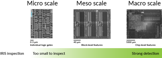
Above: Various size scales found on a chip, in relationship to IRIS capabilities.
IRIS cannot inspect the smallest features of a chip. The diagram above illustrates the various size scales found on a chip and relates it to the capabilities of IRIS. The three general feature ranges are prefixed with micro-, meso-, and macro-. On the left hand side, “micro-scale” features such as individual logic gates will be smaller than a micron tall. These are not resolvable with infra-red wavelengths and as such not directly inspectable via IRIS, so the representative image was created using SEM. The imaged region contains about 8 individual logic gates.
In the middle, we can see that “meso-scale” features can be constrained in size and identity. The representative image, taken with IRIS, shows three RAM “hard macros” in a 55 nm process. Individual row sense amplifiers are resolvable in this image. Even in a more modern sub-10 nm process, we can constrain a RAM’s size to plus/minus a few rows or columns.
On the right, “macro-scale” features are clearly enumerable. The number and count of major functional blocks such as I/O pads, data converters, oscillators, RAM, FLASH, and ROM blocks are readily identified.
IRIS is a major improvement over simply reading the numbers printed on the outside of a chip’s package and taking them at face value. It’s comparable to being able to X-ray every suitcase for dangerous objects, versus accepting suitcases based solely on their exterior size and shape.
Even with this improvement, malicious changes to chips – referred to as “hardware trojans” – can in theory remain devilishly difficult to detect, as demonstrated in “Stealthy Dopant-Level Hardware Trojans” by Becker, et al (2013). This paper proposes hardware trojans that only modulate the doping of transistors. Doping modifications would be invisible to most forms of inspection, including SEM, X-Ray ptychography, and IRIS.
The good news is that the attacks discussed (Becker, 2013) are against targets that are entirely unhardened against hardware trojans. With a reasonable amount of design-level hardening, we may be able to up the logic footprint for a hardware trojan into something large enough to be detected with IRIS. Fortunately, there is an existing body of research on hardening chips against trojans, using a variety of techniques including logic locking, built in self test (BIST) scans, path delay fingerprinting, and self-authentication methods; for an overview, see “Integrated Circuit Authentication” by Tehranipoor.
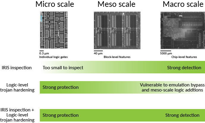
IRIS is a necessary complement to logic-level hardening methods, because logic-only methods are vulnerable to bypasses and emulation. In this scenario, a hardware trojan includes extra circuitry to evade detection by spoofing self-tests with correct answers, like a wolf carrying around a sheep’s costume that it dons only when a shepherd is nearby. Since IRIS can constrain meso-scale to macro-scale structure, we can rule out medium-to-large scale circuit modifications, giving us more confidence in the results of the micro-scale verification as reported by logic-level hardening methods.
Above: Comparison of the detection-vs-protection trade offs of logic level hardening and IRIS inspection.
Thus, IRIS can be used in conjunction with logic-level trojan hardening to provide an overall high-confidence solution in a chip’s construction using non-destructive and in situ techniques, as illustrated above.
The primary requirement of the logic-level hardening method is that it must not be bypassable with a trivial amount of logic. For example, simple “logic locking” (a method of obfuscating logic which in its most basic form inserts X(N)ORs in logic paths, requiring a correct “key” to be applied to one input of the X(N)ORs to unlock proper operation) could be bypassed with just a few gates once the key is known, so this alone is not sufficient. However, a self-test mechanism that blends state from “normal runtime” mode and “self test” mode into a checksum of some sort could present a sufficiently high bar. In such a stateful verification mechanism, the amount of additional logic required to spoof a correct answer is proportional to the amount of state accumulated in the test. Thus, one can “scale up” the coverage of a logic-level test by including more state, until the point where any reliable bypass would be large enough to be detected by IRIS (thanks to jix for pointing me in the right direction!). The precise amount of state would depend on the process geometry: smaller process geometries would need more state.
Under the assumption that each extra bit would imply an additional flip flop plus a handful of gates, a back-of-the-envelope calculation indicates a 28 nm process would require just a few bits of state in the checksum. In this scenario, the additional trojan logic would modify several square microns of chip area, and materially change the scattering pattern of infra-red light off of the chip in the region of the modification. Additional techniques such as path delay fingerprinting may be necessary to force the trojan logic to be spatially clustered, so that the modification is confined to a single region, instead of diffused throughout the standard cell logic array.
Summary and Future Direction
IRIS is a promising technique for improving trust in hardware. With a bit of foresight and planning, designers can use IRIS in conjunction with logic hardening to gain comprehensive trust in a chip’s integrity from micro- to macro-scale. While the technique may not be suitable for every chip in a system, it fits comfortably within the parameters of chips requiring high assurance such as trust roots and secure enclaves.
Of course, IRIS is most effective when combined with open source chip design. In closed source chips, we don’t know what we’re looking at, or what we’re looking for; but with open source chips we can use the design source to augment the capabilities of IRIS to pinpoint features of interest.
That being said, I’m hoping that IR-capable microscopes become a staple on hardware hacker’s workbenches, so we can start to assemble databases of what chips should look like – be they open or closed source. Such a database can also find utility in everyday supply chain operations, helping to detect fake chips or silent die revisions prior to device assembly.
Over the coming year, I hope to improve the core IRIS technique. In addition to upgrading optics and adding image stitching to my toolbox, digitally controlling the angle and azimuth of incident light should play a significant role in enhancing the utility of IRIS. The sub-wavelength features on a chip interact with incident light like a hologram. By modifying the azimuth and angle of lighting, we can likely glean even more information about the structure of the underlying circuitry, even if they are smaller than the diffraction limit of the system.
A bit further down the road, I’d like to try combining IRIS with active laser probing techniques, where IRIS is used to precisely locate a spot that is then illuminated by an intense laser beam. While this has obvious applications in fault induction, it can also have applications in verification and chip readout. For example, the localized thermal stimulation of a laser can induce the Seeback effect, creating a data-dependent change in power consumption detectable with sensitive current monitors. I note here that if physical tamper-resistance is necessary, post-verification a chip can be sealed in opaque epoxy with bits of glitter sprinkled on top to shield it from direct optical manipulation attacks and evil-maid attacks. However, this is only necessary if these attacks are actually part of the threat model. Supply chain attacks happen, by definition, upstream of the end user’s location.
The other half of optical chip verification is an image processing problem. It’s one thing to have reference images of the chip, and it’s another thing to be able to take the image of a chip and compare it to the reference image and generate a confidence score in the construction of the chip. While I’m not an expert in image processing, I think it’s important to at least try and assemble a starter pipeline using well known image processing techniques. A turnkey feature extraction and comparison tool would go a long way toward making IRIS a practically useful tool.
Ultimately, the hope is to create a verification solution that grows in parallel with the open source chip design ecosystem, so that one day we can have chips we can trust. Not only will we know what chips are intended to do, we can rest assured knowing they were built as intended, too.


