The Factory Floor, Part 2 of 4:
On Design for Manufacturing

January 14th, 2013

Akiba has new posts covering day 3 and day 4 of my “geek tour” course for MIT Media Lab students, held in Shenzhen, China. His website has been a little bogged down with traffic, so we’re thinking about migrating to a different server. Unfortunately, being inside the GFW (the Great Firewall of China) makes administering anything in the cloud a challenge.

Anyways, here’s the second installment of my four-part series titled “The Factory Floor”.

Process optimization: design for manufacturing and test jigs

It’s time to visit the topic of yield. This is a boring subject for many engineers, but for entrepreneurs, success or failure will be determined in part by achieving a reasonable yield. Unlike software, every copy of a physical good will have slight imperfections. Sometimes the imperfections will cancel out; and sometimes the imperfections gang up and degrade performance. As production volume ramps, these corner cases start adding up and a certain fraction of product ends up non-salable. In a robust design, the failing fraction may be so small that functional tests can be simplified, leading to further cost reductions. In contrast, designs sensitive to component tolerances will require extensive testing, and will suffer heavy yield losses. Reworking the defective units incurs extra labor and parts charges, ultimately leading to profit erosion.

Thus, a major challenge of moving from the engineering bench to mass production is re-designing to improve robustness in the face of normal manufacturing tolerances. This is called “design for manufacturing”, or DFM.

Examples of tolerances to consider during the design process include:

  • Passive component tolerances (i.e. resistance +/- 5%, capacitance +80/-20%, etc.)
    Spec sheet parameters that vary widely (such as hFE for bipolar transistors, Vt for FETs, Vf for LEDs). Always read the datasheet and keep an eye out for parameters that have a wide min-max spread. For example, the min-max on hFE for Fairchild’s 2N3904, ranges from 40 to 300, and the Vf on a superbright LED from Kingbright goes between 2 and 2.5V.
  • Voltage margins – particularly important for capacitors and input networks. As a rule of thumb, I try to spec capacitors with 2x headroom over nominal voltage, so I will try to use 10V caps for 5V rails and 6.3V caps for 3.3V rails. For example, many ceramic capacitor dielectrics reduce or derate their capacitance with increasing voltage. This means that ceramic capacitors in designs operating near their rated max voltage will see all the operating capacitances cornering toward the negative end of their tolerance range. Also, input networks – anything a user can plug something into – are subject to punishing ESD and other transient abuses, and special attention needs to be paid there to achieve the desired reliability.
  • PCB trace widths and layer stack variations – impacts systems requiring matched impedance, or dealing with high currents.
  • Mechanical tolerances – a case designed to fit a PCB with zero tolerance will result in the factory forcing PCBs into the case half the time, when either the PCB was cut a little large or the case came out a little small. This can lead to unintentional mechanical damage of the circuitry or the case.
  • Cosmetic blemishes – any manufactured product is subject to small blemishes, such as dust trapped in plastics, small scratches, sink marks, and abrasions. It’s important to work out the acceptance criteria for such defects ahead of time – i.e., not more than two dot blemishes larger than 0.2mm per unit, no scratch longer than 0.3mm, etc. so that the process can be crafted to avoid such defects, as opposed to the more expensive alternative of just building units and throwing away the ones that don’t meet a set of criteria imposed late in the game. Of course, nothing comes for free – to do things on the cheap, avoid high-gloss finishes and consider using matte/textured finishes that naturally hide blemishes.

DFM Improves the Bottom Line
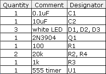
Let’s return to our LED blinker case study from part 1 of the series. Let’s say the prototype design calls for an array of three LEDs in parallel, each with its own current-set resistor. As noted above, Vf , the forward bias voltage of an LED at a given brightness, can vary by perhaps 20% between devices – in this case, from 2.0 to 2.5V. A design that uses resistive current limiting will amplify this variation. This is because an efficient circuit would drop a minority of the voltage across the current limiting resistor, leaving the parameter that sets the current – the voltage drop across the resistor – more sensitive to the variation in Vf. Since the brightness of an LED is proportional to the current flowing through the LED – not the voltage – the use of resistive current limiting to set LED brightness can lead to jarring inconsistencies in LED brightness uniformity.

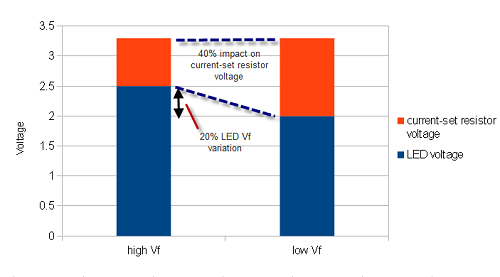
The above chart illustrates how a 20% LED Vf variation leads to a 40% change in the voltage across a current-set resistor for a fixed 3.3V supply, which will in turn lead to a 40% change in the current flowing through the LED, finally manifesting as a 40% change in perceived brightness.

Such a design may work well most the time – the problem is only pronounced when by chance a high Vf unit is paired with a low Vf unit. So for the one or two units prepared on the lab bench, things looked great.. However, a meaningful fraction of units may have brightness uniformities so bad there is choice but to reject the units. Given that most large hardware businesses have to survive on lean margins, losing even 10% of finished goods to defectivity is a terrible outcome.

One stop gap is to re-work the failed material. A factory can identify the LED that is too dim or too bright in an array, and replace it with a new one that may have a better chance of matching its cohorts. However, this rework drives up costs, and results in an unexpected and unpleasant invoice at the 11th hour of a manufacturing program. Naïve designers may be inclined to blame the factory for poor quality and argue over who should bear the cost, but it’s better to proactively avoid these kinds of problems by subjecting every design to a DFM check, and using a small pilot run to sanity-check yield before punching out a whole bunch of units.

The cost of yield fallout quantifies how much money to spend on extra circuitry to compensate for normal component variability. For example, a $10 COGS product that is yielding 80% good units has an effective cost per salable unit of $12.5 (calculated using COGS x total units built / yielded units). Therefore, increasing the COGS by $2.5 to improve yield to 100% breaks even, and spending $1 to improve yield to 99% improves the bottom line by $1.38.

In the case of the LED flasher, the dollar could be spent on a current-feedback boost regulator IC, allowing the LEDs to be stacked in series instead of parallel, so that each LED is guaranteed to have a consistent and identical amount of current flowing through them, thereby leading to greatly improved lighting uniformity. While the cost of the boost regulator is much greater than the penny spent on three current limiting LEDs, the improvement in manufacturing yield more than pays for the extra component costs.

Test for Success
The other often-neglected responsibility of a designer is the test program. A factory can only detect the problems they are instructed to look for. Therefore, every feature must be tested, no matter how trivial. For example, on a chumby device, every user-facing feature had an explicit factory test – LCD, touchscreen, audio, microphone, all the expansion ports (USB, audio), battery, buttons, knobs, etc. etc. Even the simplest buttons had to be tested. While it’s tempting to skip testing such simple components, I guarantee if it’s not tested, it will lead to returns.

And no, do not outsource the test program to the factory, even if they offer the service. First of all, the factory often doesn’t understand your design intent, so their test programs will either be inefficient, or they will test for the entirely wrong behavior. Also, factories have an incentive to pass as much material as possible, as quickly as possible, so factory-created test programs tend to be primitive and inadequate.

As a rule of thumb, for every product you make, you’re actually making two related products: one for the end user, and a test for the factory. In many ways, the test for the factory has to be as user-friendly and foolproof as the product itself – after all, tests are not run by electrical engineers. However, the related testing product will be much quicker and faster to build if adequate testability features are designed into the consumer product.

Here are some guidelines when it comes to designing a test program:

  • Strive for 100% feature coverage. It’s often easy to overlook simple or secondary features – status LEDs, an internal voltage sensor, etc. As a sanity check, look at the device and list every way a consumer can interact with the device. Ask if the test program addresses every interaction surface, if even superficially – is every LED lit, every button pressed, every sensor stimulated and every memory device touched. If the product has a microcontroller, it’s also helpful to review which drivers are loaded to cross-check the test list. Finally, do a schematic review and look at every port and consider key internal nodes to monitor as part of the test.
  • Minimize incremental setup effort. In other words, optimize the amount of time required to set up the test for each unit. This is often done through jigs that employ pogo pins or pre-aligned connector arrays. A test that requires an operator to manually probe test a dozen test points or insert a dozen connectors is time consuming and prone to manual error. Most factories in China can help design the jig for a nominal cost, but jig design is easier and more effective if the design is provisioned with adequate test points.
  • Automate test execution in a linear execution flow. Ideally, a test just run with a single button press, and then produce a pass/fail result. In practice, there will always be stop points that require operator intervention. An example of too much intervention is requiring an operator to key in or select an SSID from a list every time during a test for wifi connectivity. Instead, fix the test target SSID and hard-code that value into the test script so that the connection cycle is automatic.
  • Use icons and colors to communicate with operators, not text. Not every operator is guaranteed to be literate in a given language.
  • Employ audit logs. Record test results correlated to device serial numbers by incorporating a barcode scanner into the test rig. An alternative is to create a “test coupon” or a locally stored audit log to prove which units have had the test run successfully. This gives some hints as to what went wrong when a consumer returns a failed product. It also gives a quick method to check that the test procedure is being executed on all products. After an eight-hour shift of running test, an operator is prone to making mistakes, such as putting a defective unit accidentally into the good units’ bin. Having a quick way to check that every product that ships has been subjected to and passed the full test can help identify and isolate such problems.
  • Provide an easy update mechanism. Like any program, test programs also have bugs, and tests also need to evolve as the product has patches and upgrades applied . Thus it is imperative to have a mechanism to update and fix test programs without having to visit the factory every time in person. Many of my test fixtures have a mode where they can “phone home” via a VPN where I can then ssh into the jig itself to fix bugs: even my simplest jigs employ a linux laptop at its core.

The guidelines above are easy to implement if the product is designed with testability in mind. As most of the products I design run Linux, I leverage the processor inside the product itself to run the majority of the tests and manage the test UI. For products that lack user interaction surfaces, I will use an Android phone or a laptop connected via wifi or serial as the test UI.

Testing vs. Validation
Production tests are meant to check for assembly errors, not parametric variations or design issues. If a test is screening out devices because of normal parametric component variations, either buy better components, or re-do the design.

For consumer-grade products, there is no need to run a five minute comprehensive RAM test on every unit – in theory, a product should be designed well enough that if it’s all soldered together correctly, the RAM will do its job. A quick test to check that there are no stuck or open address pins is all that is really need. Name-brand chip vendors have typically very low defectivity rates, so we’re not validating the silicon; rather, we are validating the solder joints, connectors, and checking for missing or swapped components (note that if you buy clone chips or off-brand/remarked/partially tested devices to cut costs, it is advised to make a mini-validation program for those components).

To illustrate the point, let’s consider testing vs. validation for a switch.

A production test for a switch on a product may simply consist of asking the operator to hit the switch a few times and verify that the feel is right, and verify that electrical contact is made through a simple digital indicator.

A validation test for a switch may consist of taking a few devices, measuring contact resistance with a five-digit multimeter, subjecting them to 100% humidity at 40C overnight, and then putting the devices into an automated jig where the switches are cycled ten thousand times. Finally, the switches are re-measured with a five-digit multimeter and any degradation in close-state contact resistance is noted.

Clearly, this level of validation cannot be performed on every device manufactured. Rather, the validation program checks for performance of the switch over the expected lifetime of the product, and the test just makes sure the switch is put together right. Note that it is considered good practice to re-run validation tests on a couple randomly sampled units out of every several thousand units produced; there are formulas and tables to compute how much sampling is needed to achieve a certain level of quality.

So how much testing is enough testing? One threshold for testing can be derived through a cost argument. Every additional test run incurs test equipment costs, engineering costs, and the variable cost of the test time. As a result, testing is subject to diminishing returns: at some point, it’s cheaper just to take a product return than to test more. Naturally, the testing bar is much higher for medical or industrial grade equipment, as the liability associated with faulty equipment is also much higher. Likewise, a novelty product meant to be given away may get away with much less testing.

As a final thought, don’t dismiss the value of applying solid engineering to test jig design. I once had a problem once where a flat flex cable adapter with 50 pins had random cold solder joint failures. I asked the factory to build a test to validate the adapters. Their solution was to hang LEDs off of every pin of the adapter and put a test voltage into one side, and look for LEDs that don’t light up on the other side. The problem is that the cold solder joints weren’t simply open or closed – some were just high resistance. Enough current would flow to light an LED, yet enough resistance would be present to cause a fault in the design. After I noted this problem, the factory proposed buying 50 multimeters and hanging them off of every pin to check the resistance manually – an expensive and error-prone proposition. My response was to daisy-chain the connections across the adapter, and then use a single multimeter to check the net resistance of the daisy chain. Putting the connections in series checks all 50 connections with a single numeric measurement (as opposed to the subjective observation of an LED’s brightness). As one can see, even a test as simple as checking for cold solder joints on a cable adapter can have better or worse implementations. As ever more complicated components require ever more subtle tests, there is real value in applying solid engineering skills to crafting efficient yet foolproof tests.

Updates from the Tour in China

January 9th, 2013

Akiba is providing a running commentary of the MIT Media Lab IAP China immersion experience. If you’re curious about it, check it out. So far he has day 1 and day 2 up.

Above is a photo of Colman Lee, a mechanical designer from AQS, lecturing the students about some of the more subtle aspects of mold and tool design. AQS is my go-to manufacturing services partner / general problem solving crew, and they helped with many of the local arrangements for the trip. Below is a group photo at Colinda, our first stop on the tour where we got to take a look inside the Onyx Geiger counter injection molding tool.

The Factory Floor, Part 1 of 4:
The Quotation (or, How to Make a BOM)

January 5th, 2013

This month, I will be teaching a few MIT Media Lab graduate students and doing a bit of a “geek tour” of Shenzhen – we will visit several factories and live among the electronic markets to facilitate new directions and expand horizons in the students’ hardware-oriented research projects.

As part of the course, they will learn how to scale up their research utilizing the China manufacturing ecosystem. These lessons may also be useful for Makers looking to bootstrap a product in moderate volumes (hundreds to thousands of units). I will share some tips and insights from the course in four posts over the next month covering:

  • Getting a quotation: documentation standards (how to make a BOM)
  • Process optimization: design for manufacturing and test jigs
  • Industrial design for startups: guerrilla engineering on a shoestring budget
  • How to pick a factory: building and maintaining partnerships

Part 1 of 4: The Quotation (or, How to Make a BOM)

Most Makers trying to scale up quickly realize the only practical path forward is to outsource production. If only outsourcing were as easy as schematic + cash = product! Whether working with the assembly shop down the street or going to China, a clear and complete bill of materials (BOM) is the first step to outsourcing production.

Every single assumption, down to the color of the soldermask, has to be spelled out unambiguously for a third party to faithfully reproduce a design. Missing or incomplete documentation is the lead cause of production delays, defects, and cost overruns. So, we will start the series on the topic of making a complete and accurate BOM for quotation.

Let’s consider a simple case study. Suppose we Kickstarted a bicycle safety light. It contains a circuit using the 555 timer to flash a small array of LEDs. After a great marketing campaign, we now have to fill several hundred orders in a few months’ time.

At this point, here’s how the starting BOM might look:

This BOM, along with a schematic, is likely sufficient for an engineer to reproduce the prototype, but this is far from adequate for a manufacturing cost quotation. Here’s some of the things missing from the BOM:

  • Approved manufacturer for each component
  • Tolerance, material composition, and voltage spec for passive components
  • Package type information for all parts
  • Extended part numbers specific to each manufacturer

Furthermore, the table above addresses only the electronics BOM. A complete BOM for an LED flasher also needs to include the PCB, battery, plastic case pieces, lens, screws, any labeling (for example, a serial number), a manual, and packaging (plastic bag plus cardboard box, for example). There may also need to be a master carton as a single boxed LED flasher is too small to ship on its own. Although cardboard boxes are cheap, they aren’t free, and if they aren’t ordered on time, inventory will sit on the dock until a master carton is delivered for final pack-out prior to shipment.

Here’s a little more about each of the missing items from the example BOM.

Approved manufacturers

A proper factory will require the allowed manufacture(s) to be specified for every part. This is frequently referred to as the “AVL”, or Approved Vendor List. A manufacturer is not a distributor (i.e., Digikey, Mouser, Avnet); a manufacturer is the actual company that makes the part. A capacitor, for example, could be made by TDK, Murata, Taiyo Yuden, AVX, Panasonic, Samsung, etc. You’ll be surprised how many times I’ve reviewed a BOM listing “Digikey” or some other distributor as the manufacturer for a part.

While it may seem silly to trifle over who makes a capacitor, there are definitely situations in which the maker of a component matters – even for the humble capacitor. For example, blindly substituting the filter capacitors on a switching regulator, even if the substitute has the same rated capacitance and voltage, can lead to unstable operation and even boards catching fire.

Of course, there are times when one is truly insensitive to the manufacturer, in which case I would mark on the BOM “any/open” for the AVL (particularly true for things like pull-up resistors). This invites the factory to suggest their preferred supplier on your behalf.

Tolerance, composition, and voltage spec

For passive components that are marked as “any/open”, there are some key parameters that should always be specified in a BOM to ensure the right part is purchased:

  • For resistors, at a minimum the tolerance and wattage should be specified. A 1k, 1% 1/4W carbon resistor is very different beast from a 1k, 5% 1W wirewound resistor!
  • For capacitors, at a minimum the tolerance, voltage rating, and dielectric type should be specified. For special applications, certain parameters such as ESR or ripple current tolerance also need to be specified. A 10uF, electrolytic, 10% 50V capacitor has vastly different performance at high frequencies compared to a 10uF, X7R [ceramic], 20% 16V capacitor.
  • Inductors are sufficiently specialized that it’s not recommended to ever leave them as “any/open”. For power inductors, core composition, DCR, saturation, temperature rise current, are the basic parameters, but there is also no standard for casing like there is for resistors and capacitors. Furthermore, important parameters such as shielding and potting, which can have material impacts on the performance of a circuit, are often implicit in a part number; hence, it’s best to simply fully specify the inductor and not leave it any/open. The same goes for RF inductors.

Electronic component form factor

It’s always important to fully specify the form factor, or “package type”, of a component. Poorly specified or under-specified package parameters can lead to assembly errors. Beyond the basic parameters such as the EIA or JEDEC package code (0402, 0805, TSSOP, etc.), here are some other things to consider:

  • For SMT packages, the height of a component can vary, particularly for packages larger than 1206, or inductors. Pay attention if the board is slotting into a tight case.
  • For through-hole packages, lead pitch and component height should always be specified.
  • For ICs, try to specify the common name that corresponds to the package, not just the manufacturer’s internal code (for example, a TI “DW” type package code corresponds to SOIC). It’s a good consistency check that can guard against errors.

Extended part numbers

Designers often think using abbreviated part numbers. A great example of this is the 7404. The venerable 7404 is a hex inverter, and has been in service for decades. Because of its ubiquity, the term “7404” can be used as a generic term for an inverter. However, when going to production, things like the package type, manufacturer and logic family must be specified. A complete part number might be 74VHCT04AMTC, which specifies an inverter made by Fairchild Semiconductor, from the “VHCT” series, in a TSSOP package, shipped in tubes. The extra characters are very important, because small variations can lead to big problems, such as quoting and ordering the wrong packaged device (and subsequently being stuck with a reel of unusable parts), or subtle reliability problems. In fact, I encountered a problem once due to a mistaken substitution of a “VHC” for the “VHCT” logic family part. This switched the input thresholds of the inverter from TTL to CMOS logic-compatible, and resulted in some units having an asymmetric response to input signals. Fortunately, I caught this problem before production ramped, avoiding a whole lot of potential rework or worse yet, returns.

Here’s another example of how missing a couple of characters can cost thousands of dollars. A fully specified part number for the LM3670 switching regulator might be LM3670MFX-3.3/NOPB. Significantly, if the /NOPB is omitted, the part number is still valid and orderable – but for a version that uses leaded solder. This could be disastrous for products exporting to a region, such as the EU, that requires RoHS compliance (meaning lead-free, among other things). A more subtle issue is the “X” in the part number. Part numbers with an “X” come with 3,000 pieces to a reel, and ones lacking an “X” come in 1,000 pieces to a reel. While many factories will question the /NOPB omission (since factories typically assemble RoHS documentation as they purchase parts), they will rarely flag the reel quantity as an issue. However, you care about the reel quantity because if you only wanted 1,000 pieces, including the X in the part number means you’ll be paying for 2,000 extra pieces you don’t need. Or, if you’re doing a much larger production run and you omit the X, you could be paying a premium for shipping three times the volume of reels for the same purchase quantity. Either way, the factory will quote the part exactly as specified, and you could be missing out on a cost savings if you’re not paying attention to the reel quantities.

The bottom line is that every digit and character counts, and lack of attention to detail can cost real money!

BOM Revisited

Here’s an example of how a proper, fully-specified BOM for quotation of the same project example above would look.


(click for a larger version, or get the original in open office format here)

Note that the BOM above doesn’t call out factory margin, labor for assembly, pack-out, shipping, duties, etc. These “soft costs” will be discussed in the final post of the series. However, it’s important to note that when building a business model, parts cost is not the only cost to consider — the above BOM just gets you started with the initial quotation process.

Let’s compare this to our original BOM for contrast:

There is big difference between a BOM that any engineer could take to produce a prototype, and a BOM that any factory could take to mass-produce a product.

Note that two additional columns have crept into the final BOM, the “MOQ” (minimum order quantity) and the “lead time”. These columns are irrelevant when building low-volume prototypes, as one would typically buy parts from distributors which have few MOQ restrictions and maintain stock on hand for next-day deliveries. However, when scaling into production, a big cost savings are realized by cutting the distributor overhead and buying through wholesale channels. In wholesale channels, MOQs and lead times matter.

The good news is the factory will fill in the MOQ and lead time as part of the quotation process. However, these are parameters that are helpful to be tracked from the beginning of a design. If the MOQ of a particular component is very high, one may have to buy massive numbers of excess parts which increases the effective price of the project. If the lead time of a part is very long, one may want to consider redesigning for a part with a shorter lead time. Using parts with shorter lead times not only saves time, it improves cash flow, as the last thing anyone wants to do is tie up cash on long-lead components 4 months in advance of any sales revenue.

Also note the inclusion of all the “miscellaneous” bits for the design inside the BOM, left out on the engineering prototype’s BOM. The miscellaneous bits are easy to forget, but a missing user manual in an initial BOM is often times not discovered until opening the final sample for approval, leading to a last-minute scramble to get it into the final product. Many, many products have been delayed or late simply because a user manual or box art was not completed and approved in time, and it sucks to have a hundred thousand dollars worth of inventory idling in a warehouse for want of a slip of paper.

Finally, it’s best practice to provide the factory with “golden samples” along with CAD files. These prototypes enable the factory to make smarter decisions about any ambiguities in the submitted BOM. It may suck to hand-solder together one more unit just for the factory, but in my opinion a few hours of soldering beats a week of trading clarifying emails with the factory.

Coping with Change

Designs change. Even if a design is perfect, sometimes vendors End-of-Life (EOL) components, forcing a change to the design. And let’s face it, not all design assumptions survive contact with real consumers. While the quotation process is fluid, it’s important to formalize the change process once crossing the threshold into production. It is best practice to use a written, formal Engineering Change Orders (ECO) to update the factory on any changes after the initial quotation is completed. An ECO template should have at a minimum the documentation detailing each part changed and brief explanation of why, along with a unique revision number for conveniently referencing the change down the road, and a method to record the factory’s receipt of the ECO paperwork. Failing to be thorough about ECOs and relying on casual emails will often lead to buyers buying the wrong part, or worse yet the factory installing the wrong part and entire lots being scrapped or reworked. Even after troubleshooting a problem with the factory engineers, I will still write up a formal ECO and submit it to the production staff to formalize the findings. I hate paperwork as much as the next engineer, but in production one small mistake can cost tens of thousands of dollars, and that thought keeps me disciplined on ECOs.

Stay tuned for next week when I cover design for manufacturing and test jigs.

Sifteo Gen2: from Concept to Product

December 17th, 2012

Some readers may have already seen this, but adafruit has a great article written by Sifteo engineer Elizabeth Micah Scott about the challenges and trade-offs they encountered bringing their Gen2 product to market (full disclosure: I am an advisor for Sifteo).


I really appreciate the candidness of the writing, and the openness with which they discuss internal design aspects that many startups would normally regard as highly secret sauce. Then again, they do some amazingly clever things with very light, cheap 8-bit hardware, and they have every right to be proud of their technical accomplishments.


Sifteo has an SDK for those interested in developing for the platform.

I highly recommend the read, check out the article titled “How we built a Super Nintendo out of a Wireless Keyboard @Sifteo” here.

Building my Own Laptop

December 16th, 2012

We are building an open laptop, with some wacky features in it for hackers like me.

This is a lengthy project. Fortunately, ARM CPUs are getting fast enough, and Moore’s Law is slowing down, so that even if it took a year or so to complete, I won’t be left with a woefully useless design. Today’s state of the art ARM CPUs — quad-core with GHz+ performance levels — is good enough for most day-to-day code development, email checking, browsing etc.

We started the design in June, and last week I got my first prototype motherboards, hot off the SMT line. It’s booting linux, and I’m currently grinding through the validation of all the sub-components. I thought I’d share the design progress with my readers.

Of course, a feature of a build-it-yourself laptop is that all the design documentation is open, so others of sufficient skill and resources can also build it. The hardware and its sub-components are picked so as to make this the most practically open hardware laptop I could create using state of the art technology. You can download, without NDA, the datasheets for all the components, and key peripheral options are available so it’s possible to build a complete firmware from source with no opaque blobs.

Above is an annotated diagram of the circuit board. The dimensions of the board are approximately 121mm x 150mm — sized to fit comfortably underneath a standard-sized laptop keyboard. The image above is rotated versus the installation orientation; the port farm is meant to be on the right hand side of the laptop, not on the bottom. The overall height of the board is just under 14mm, with the height being set by the thickness of an Ethernet connector. The thickness on my Lenovo T520 base portion is just under 24mm, so once we stack a keyboard and plastics on this it’ll be just about the same.

Here are some of the features of the laptop motherboard:

  • Freescale iMX6 CPU — same footprint can support dual-lite and quad versions:
  • Internal memory:
    • Boot from microSD firmware
    • 64-bit, DDR3-1066 SO-DIMM, upgradable to 4GB
    • SATA-II (3Gbps)
  • Internal ports & sensors:
    • mini PCI-express slot (for blob-free wifi, bluetooth, mobile data, etc.)
    • UIM slot for mPCIe mobile data cards
    • Dual-channel LVDS LCD connector (up to QXGA (2048×1536) @ 60Hz resolution) with USB2.0 side-channel for a display-side camera
    • Resistive touchscreen controller (note: captouch displays typically come with a controller)
    • 1.1W, 8-ohm internal speaker connectors
    • 2x USB2.0 internal connectors for keyboard and mouse/trackpad
    • Digital microphone
    • 3-axis accelerometer
    • header for optional AW-NU137 wifi module (*)
  • External ports:
    • HDMI
    • SD card reader
    • headphone + mic port (compatible with most mobile phone headsets, supports sensing in-line cable buttons)
    • 2x USB 2.0 ports, supporting high-current (1.5A) device charging
    • 1Gbit ethernet
  • “Fun” features:
    • 100 Mbit ethernet — dual Ethernet capability allows laptop to be used as an in-line packet filter or router
    • USB OTG — enables laptop to spoof/fuzz ethernet, serial, etc. over USB via gadget interface to other USB hosts
    • Utility serial EEPROM — for storing crash logs and other bits of handy data
    • Spartan-6 CSG324-packaged FPGA — has several interfaces to the CPU, including a 2Gbit/s (peak) RAM-like bus — for your bitcoin mining needs. Or whatever else you might want to toss in an FPGA.
    • 8x FPGA-driven 12-bit, 200ksps analog inputs
    • 8x FPGA-driven digital I/O
    • 8x FPGA-driven PWM headers, compatible with hobby ESC and PWM pinouts — enables direct interfacing with various RC motor/servo configurations & quad-copter controllers
    • Raspberry-Pi compatible expansion header
    • 13x CPU-driven supplemental digital I/Os
    • 3x internal UART ports

    Items marked with an asterisk (*) require a closed-source firmware blob, but the system is functional and bootable without the blob.

    In order to give maximum power management flexibility, the battery interface functions are implemented on a daughtercard. I co-opt a cheap and common SATA-style connector to route power and control signals between the mainboard and the daughtercard. To prevent users from accidentally plugging a hard drive into the battery port, I inverted the gender of the battery-SATA connector from the actual mass storage SATA-II connector. The current battery card is meant to work with the battery packs used by most RC enthusiasts — LiPo packs ranging from 2S1P to 4S1P (2-cell to 4-cell). RC packs are great because they are designed for super-fast charging. They are also cheap and easy to buy. For the board-side battery plug I decided to use the Molex connector found on classic disk drives, since they are cheap, common, and easy to assemble with simple tools. I couldn’t use a standard RC connector because the vast majority of them are designed for in-line use, and the few that have board mounts are too thick or too weird for use in this application.

    The battery board can charge batteries at rates in excess of 4A. This means charging a 3-cell, 45Wh (4Ah) pack in about one hour. I’m estimating that a typical power consumption for a reasonable system configuration might be around 5-6W, so that’s 7-8 hours of runtime with a 1-hour charge time using that type of battery pack. Of course, since the whole laptop is user-configurable, typical power consumption is really hard to estimate — you could drop in a monster LCD and a power-hungry magnetic hard drive with loads of peripherals and the power consumption could be much higher. Of course, you can drop in a 100Wh battery pack if you wanted as well :)

    Another cute feature of the battery board is that it can drive an analog panel meter. Xobs had suggested that it would be neat to embed a retro analog needle meter into the palmrest of the laptop to give a real-time display of power consumption. I thought it was a great idea, so I designed that in. Of course, the analog meter is driven by a DAC on the battery microcontroller, so it can be configured to perform a multitude of useful (or not so useful) analog read-outs, such as remaining runtime, battery voltage, temperature, the time (represented as an analog value), etc.

    Next up is to spend a couple months validating all the features on the board — a long list of features to grind through indeed — and port drivers and a linux distro (no small task, but I’ll have Xobs‘ skillful help). I also am looking forward to designing the enclosure. Probably for the first rev, I will do something out of laser-cut acrylic that is vaguely tablet-like, to avoid having to mess around with a friction clutch on version 1 of the plastics.

    A detached keyboard/trackpoint is attractive to me because I’ve always wanted a display I can “hang” on the seat in front of mine when sitting in an airplane or a bus — it’s a lot easier on the neck and the arrangement actually works better if the person in front reclines their seat.

    Once I’ve got some experience integrating the whole thing, I’ll probably design a rev-2 case using CNC-cut ABS and aluminum. CNC cut ABS is almost as robust as injection molded ABS, and can produce reasonably intricate shapes. It’s also relatively economical to produce in single quantities. The CNC-cut design could be a clamshell design, or maybe some other funky design. Maybe I’ll try using wood and brass — who knows, the whole idea of making my own laptop is to play around with some new ideas!

    It occurs to me that maybe other people might also be interested in owning a laptop like this, but don’t want to go through the trouble of fabricating their own circuit boards. If it seems like a few hundred folks are interested, I might be convinced to try a Kickstarter campaign in several months, once the design is stable and tested. However, I’m not looking to break any low-price records for this laptop — if you just want a cheap linux laptop you’re better off buying a netbook or EeePC. This is a low-volume, hand-crafted laptop made with uniquely open-source components, so the pricing would be consistent with such crafted goods.

    For those interested in the source files for the current early prototype iteration of the design, bounce over to the Novena wiki, and keep an eye on Xobs’ blog. Novena (yet another Singaporean metro station, and also Latin for “nine”) is our stand-in codename for the laptop motherboard.