Archive for the ‘Hacking’ Category

Winner of Name that Ware February 2008!

Monday, April 7th, 2008

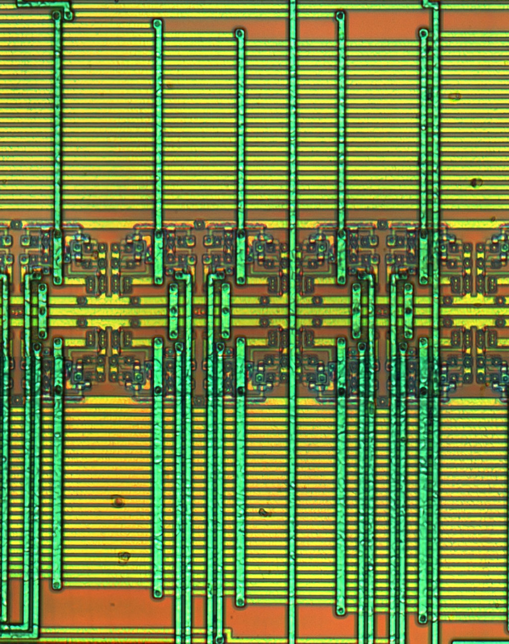
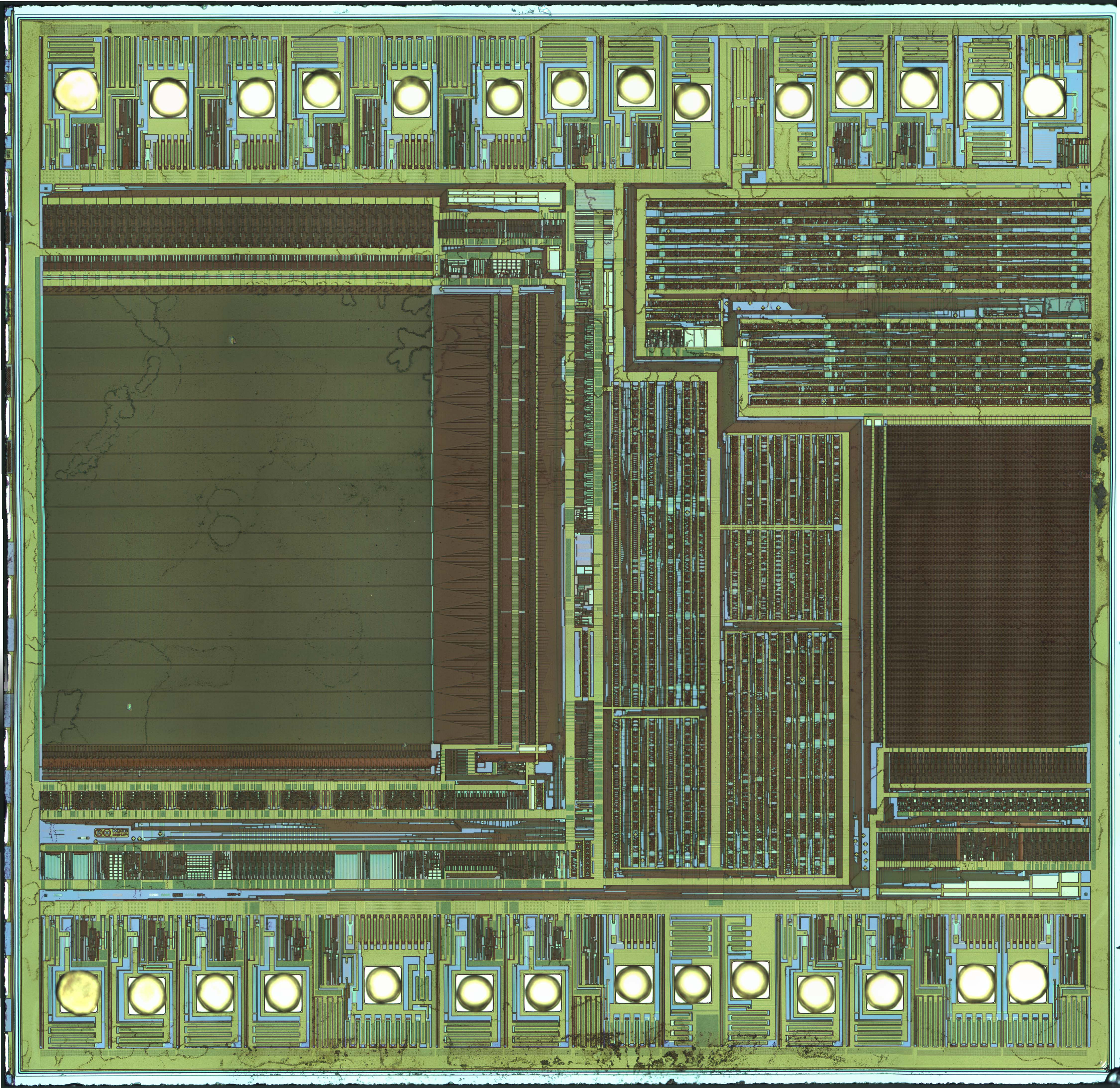
The solution to the Ware from last month is shown below. Below is the schematic overlaid on the transistors, and then the schematic redrawn in a more recognizable form, highlighting the cross-coupled inverter pair that forms the core of a typical static CMOS storage element.

In this circuit, P1/N4 form the output driver/buffer. P2/P3 form the storage pair.

A more detailed analysis including a breakout of the connectivity in the context photo can be found in this PDF file.

The basic functionality of the device is probably a pulse stretcher, depending on how it’s connected to the rest of the circuit. The device is transparent while the enable is high, and in a memory state when D is low and enable is low. If the D is driven high while the enable is driven low, the device always goes to a 1 state, and stays in that state until the enable is high again while D is low, thus stretching out the pulse.

This device is part of an array that spans a spot between the random logic array and the RF section of a MIFARE RFID reader chip, specifically the MFRC530 by NXP. My best guess is that it’s part of an array that stores/processes baseband information coming back from the RF section of the IC. Shouts to Chris and Karsten for their help at looking at this device, and especially to Flylogic for providing the awesome photos! If you like looking at chipshots and silicon security, you seriously need to check out the Flylogic blog.

The quality of the entries for last months’ contest are all very high. Unfortunately, I can’t quite declare a winner yet, because I don’t have Sii’s plaintext or sto’s plaintext. Sto’s schematics are correct, and it does call out the memory function of the device, but Sii looks like the answer might be correct, and the post is earlier than sto’s. pablot could also have a correct schematic, but since an answer wasn’t specifically named, it’s currently down to who has the correct answer between Sii and sto; if Sii’s answer is correct, Sii wins; otherwise, sto wins because of the correct schematics posted.

Thanks for playing! Post your plaintext in the comments, and the winner will be named in the comments.

Name that Ware February 2008

Sunday, March 9th, 2008

The ware for February 2008 is shown below. Click on any of the images for a larger version.

The past two Name that Wares were fairly easy, so I thought I’d make this one a little more challenging — and yes, this month I can offer again a dent-and-scratch chumby as the prize! This one involves silicon reading — for those unfamiliar with the art of reading silicon, check out May 2006’s name that ware and the primer post (has this competition really been going on for that long? I should make a picture calendar of past Name that Wares).

In the above photos, there is a single unit cell, replicated a few times, and the objective is to correctly name the function of the unit cell. There is sufficient information in the above micrographs to derive an exact schematic of the unit cell. The top photo is a zoomed-in version with all layers intact; the middle photo is a confocal image of the unit cells with all metal stripped back, revealing just the polysilicon gates. The bottom photos is an all-metal intact context photo for the unit cells. The photos are, as usual, decaped, delayered, and imaged by the skilled hands at Flylogic!

Winner of Name That Ware January 2008!

Sunday, March 9th, 2008

The ware for January 2008 was a Tangent Quattro internet radio alarm clock, and the winner is vt! Congratulations. Picking a winner, as usual, was not easy, but vt had both the most timely answer and an adequate set of follow-up explanations revealing the thought process behind the guess. Azer gets an honorable mention for using pixel scaling off of a known reference geometry (the USB plug) to determine the size of the device and narrow down the possibilities; I thought that was clever.

Some of the details of the Tangent Quattro were interesting. It’s basically a speaker that happens to have an embedded linux computer with wifi inside it — in other words, the speaker was designed first, and then the electronics were fitted around the acoustic chamber. I think that’s a good methodology for designing any integrated hi-fi device like this. On the back panel of the device is a slogan of sorts that I got a chuckle out of:

Here is a photo of the Reciva module’s front side:

Since the processor is an ARM9 architecture device, I took the liberty of reading out the ROM and mounting its JFFS2 filesystem on a chumby, and poking around a bit. It’s interesting to see their method for storing configuration information such as WEP keys, access point settings, and alarms…but I digress.

Above is a photo of the antenna they use. You might recognize it — it’s a standard 802.11 access point antenna. It’s not a terrible idea to stick with things that just work, especially if you have the space and cost headroom to afford such an antenna.

Above is a photo of the back panel CCA for the radio. The interesting part is how they implemented the 100baseT connection — it’s essentially the guts of a USB dongle laid out into the PCB (upper right hand corner of the CCA). This is an ever more popular approach, as I’m finding that USB has gotten so cheap and easy to integrate that it’s no longer just for external peripheral interconnect — it’s becoming usable as an inside-the-box interconnect standard as well.

Wii Like Chipshots!

Tuesday, February 19th, 2008

I love looking inside chips, and Flylogic takes some of the sweetest chip shots. bushing sent me some Wii chips to play with a few weeks ago, and Chris at Flylogic expertly decap’d and imaged them for me. I thought they were pretty neat, so here’s a couple of them to share with you:

The chip above is the Macronix mask ROM part inside the Wii. It also has some SRAM and a real time clock on-die. The large block on the left is the mask ROM, and the smaller block on the right is the SRAM. The top right has a fairly regular arrays of flip-flop like logic structures, so those are probably command or address registers for the chip.

The chip above is the serial EEPROM chip that’s flip-mounted onto the Hollywood package. The Hollywood GPU on the Wii actually consists of three silicon chips on a single substrate, as the image below shows. The serial EEPROM is indicated by the pink arrow.

The bond pads still have the flip-mounting bumps on them, so they show up as large black circles in the photo. Flylogic later removed the bumps using a neat hack with their wirebonder, and then rebonded the die into an 8-pin DIP so the contents could be read out with a conventional ROM burner. I found it particularly enlightening to see the ratio of logic versus the size of the actual memory array for the serial EEPROM (the memory array is the regular set of cells in the top-right corner). Essentially, at this capacity scale (2048 bits), you’re paying for a bunch of logic, and not much memory. Doubling the memory capacity would minimally impact the overall die size, since most of what’s on there looks to be flip flops for shift registers and command latches.

Name that Ware January 2008

Friday, February 8th, 2008

The ware for January 2008 is shown below. Click on the image for a much larger version.

This photograph isn’t of the whole unit, it’s just of one (important) part of it; but I think that’s part of the challenge. I believe there are enough hints buried in the photograph for one to deduce exactly what product this comes from.

This month, I will again be able to offer a dent-and-scratch chumby as a prize. Have fun!