Archive for the ‘The Factory Floor’ Category

New US Tariffs are Anti-Maker and Will Encourage Offshoring

Tuesday, June 19th, 2018

The new 25% tariffs announced by the USTR, set to go into effect on July 6th, are decidedly anti-Maker and ironically pro-offshoring. I’ve examined the tariff lists (List 1 and List 2), and it taxes the import of basic components, tools and sub-assemblies, while giving fully assembled goods a free pass. The USTR’s press release is careful to mention that the tariffs “do not include goods commonly purchased by American consumers such as cellular telephones or televisions.”

Think about it – big companies with the resources to organize thousands of overseas workers making TVs and cell phones will have their outsourced supply chains protected, but small companies that still assemble valuable goods from basic parts inside the US are about to see significant cost increases. Worse yet educators, already forced to work with a shoe-string budget, are going to return from their summer recess to find that basic parts, tools and components for use in the classroom are now significantly more expensive.


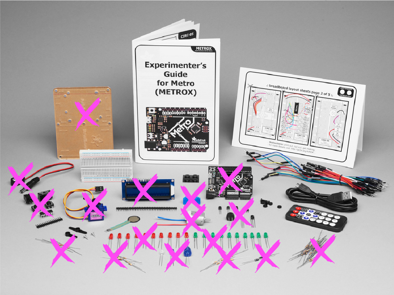
Above: The Adafruit MetroX Classic Kit is representative of a typical electronics education kit. Items marked with an “X” in the above image are potentially impacted by the new USTR tariffs.

New Tariffs Reward Offshoring, Encourage IP Flight

Some of the most compelling jobs to bring back to the US are the so-called “last screw” system integration operations. These often involve the complex and precise process of integrating simple sub-assemblies into high-value goods such as 3D printers or cell phones. Quality control and IP protection are paramount. I often advise startups to consider putting their system integration operations in the US because difficult-to-protect intellectual property, such as firmware, never has to be exported if the firmware upload operation happens in the US. The ability to leverage China for low-value subassemblies opens more headroom to create high-value jobs in the US, improving the overall competitiveness of American companies.

Unfortunately, the structure of the new tariffs are exactly the opposite of what you would expect to bring those jobs back to the US. Stiff new taxes on simple components, sub-assemblies, and tools like soldering irons contrasted against a lack of taxation on finished goods pushes business owners to send these “last screw” operation overseas. Basically, with these new tariffs the more value-add sent outside the borders of the US, the more profitable a business will be. Not even concerns over IP security could overcome a 25% increase in base costs and keep operations in the US.

It seems the intention of the new tariff structure was to minimize the immediate pain that voters would feel in the upcoming mid-terms by waiving taxes on finished goods. Unfortunately, the reality is it gives small businesses that were once considering setting up shop in the US a solid reason to look off-shore, while rewarding large corporations for heavy investments in overseas operations.

New Tariffs Hurt Educators and Makers

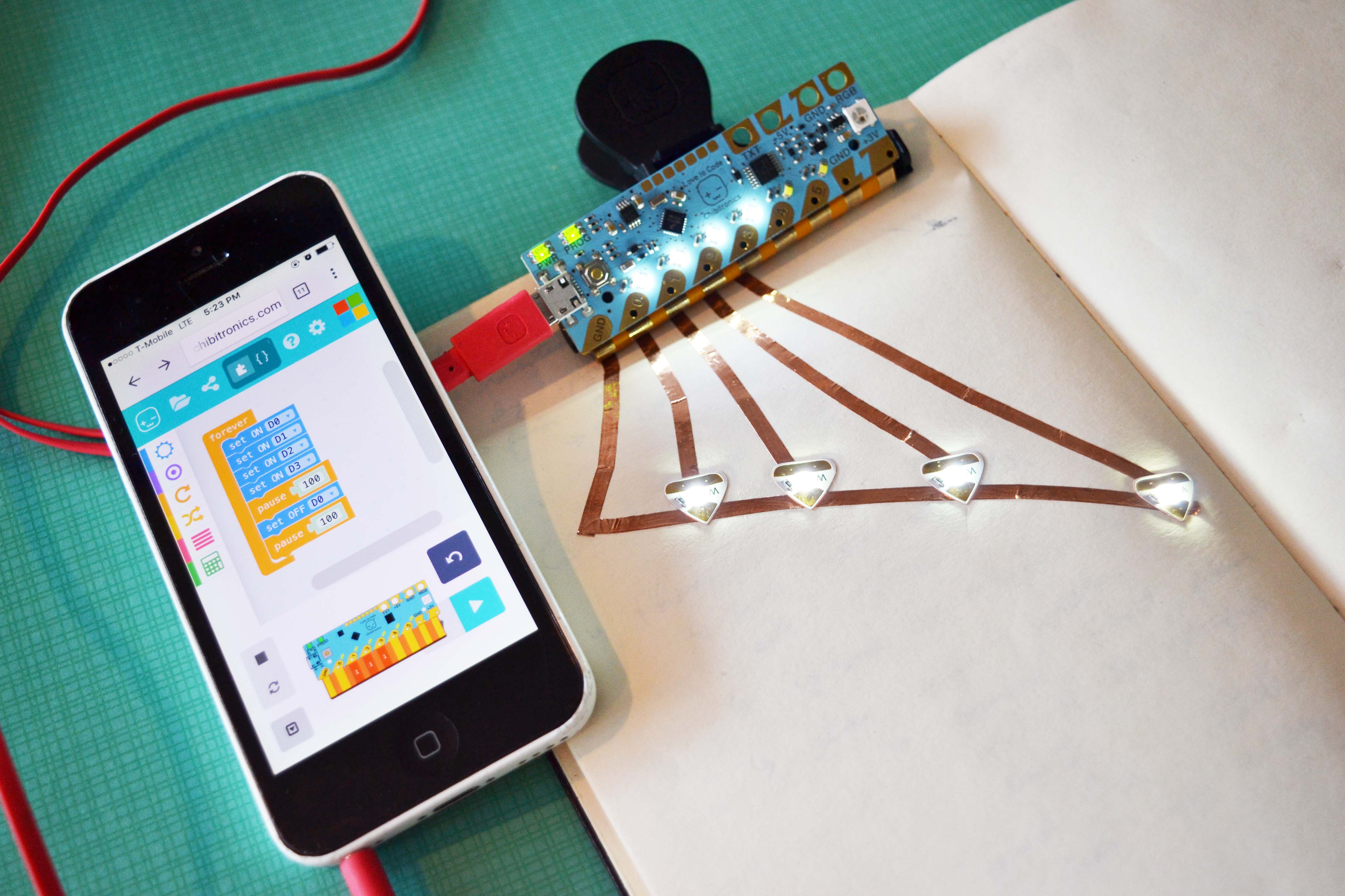
Learning how to blink a light is the de-facto introduction to electronics. This project is often done with the help of a circuit board, such as a Microbit or Chibi Chip, and a type of light known as an LED. Unfortunately, both of those items – simple circuit boards and LEDs – are about to get 25% more expensive with the new tariffs, along with other Maker and educator staples such as capacitors, resistors, soldering irons, and oscilloscopes. The impact of this cost hike will be felt throughout the industry, but most sharply by educators, especially those serving under-funded school districts.


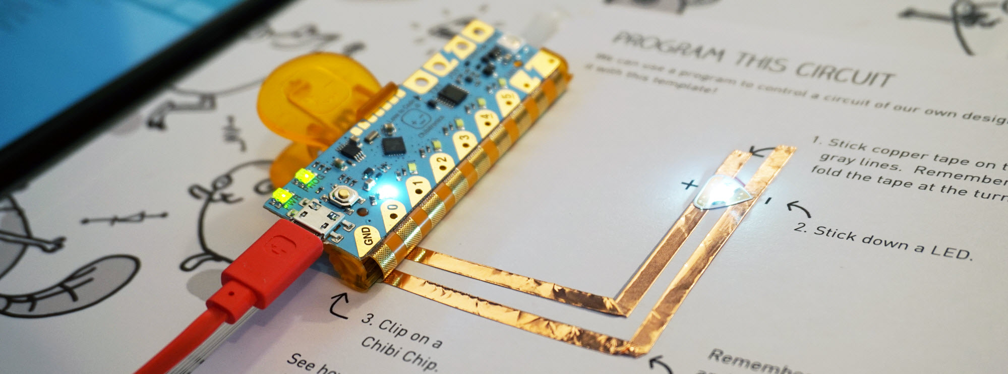
Above: Learning to blink a light is the de-facto introduction to electronics, and it typically involves a circuit board and an LED, like those pictured above.

Somewhere on the Pacific Ocean right now floats a container of goods for ed-tech startup Chibitronics. The goods are slated primarily for educators and Makers that are stocking up for the fall semester. It will arrive in the US the second week of July, and will likely be greeted by a heavy import tax. I know this because I’m directly involved in the startup’s operations. Chibitronics’ core mission is to serve the educator market, and as part of that we routinely offered deep discounts on bulk products for educators and school systems. Now, thanks to the new tariffs on the basic components that educators rely upon to teach electronics, we are less able to fulfill our mission.

A 25% jump in base costs forces us to choose between immediate price increases or cutting the salaries of our American employees who support the educators. These new tariffs are a tax on America’s future – it deprives some of the most vulnerable groups of access to technology education, making future American workers less competitive on the global stage.


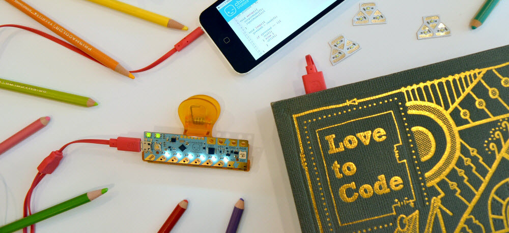
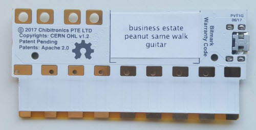
Above: Educator-oriented learning kits like the Chibitronics “Love to Code” are slated for price increases this fall due to the new tariffs.

Protectionism is Bad for Technological Leadership

Recently, I was sent photos by Hernandi Krammes of a network card that was manufactured in Brazil around 1992. One of the most striking features of the card was how retro it looked – straight out of the 80’s, a full decade behind its time. This is a result of Brazil’s policy of protectionist tariffs on the import of high-tech components. While stiff tariffs on the import of microchips drove investment in local chip companies, trade barriers meant the local companies didn’t have to be as competitive. With less incentive to re-invest or upgrade, local technology fell behind the curve, leading ultimately to anachronisms like the Brazilian Ethernet card pictured below.


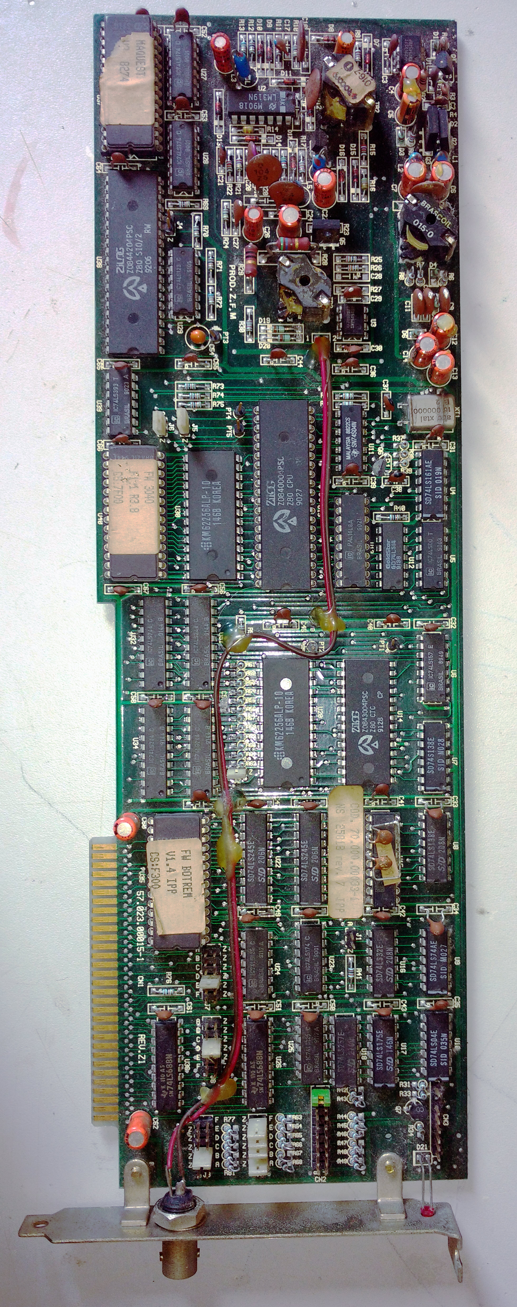
Above: this Brazilian network card from 1992 features design techniques from the early 80’s. It is large and clunky compared to contemporaneous cards.

Significantly, it’s not that the Brazilian engineers were any less clever than their Western counterparts: they displayed considerable ingenuity getting a network card to work at all using primarily domestically-produced components. The tragedy is instead of using their brainpower to create industry-leading technology, most of their effort went into playing catch-up with the rest of the world. By the time protectionist policies were repealed in Brazil, the local industry was too far behind to effectively compete on a global scale.

Should the US follow Brazil’s protectionist stance on trade, it’s conceivable that some day I might be remarking on the quaintness of American network cards compared to their more advanced Chinese or European counterparts. Trade barriers don’t make a country more competitive – in fact, quite the opposite. In a competition of ideas, you want to start with the best tech available anywhere; otherwise, you’re still jogging to the starting line while the competition has already finished their first lap.

Stand Up and Be Heard

There is a sliver of good news in all of this for American Makers. The list of commodities targeted in the trade war is not yet complete. The “List 2” items – which include all manner of microchips, motors, and plastics (such as 3D printer PLA filament and acrylic sheets for laser cutting) that are building blocks for small businesses and Makers – have yet to be ratified. The USTR website has indicated in the coming weeks they will disclose a process for public review and comment. Once this process is made transparent – whether you are a small business owner or the parent of a child with technical aspirations – I encourage you to please share your stories and concerns on how you will be negatively impacted by these additional tariffs.

Some of the List 2 items still under review include:

9030.31.00 Multimeters for measuring or checking electrical voltage, current, resistance or power, without a recording device
8541.10.00 Diodes, other than photosensitive or light-emitting diodes
8541.40.60 Diodes for semiconductor devices, other than light-emitting diodes, nesoi
8542.31.00 Electronic integrated circuits: processors and controllers
8542.32.00 Electronic integrated circuits: memories
8542.33.00 Electronic integrated circuits: amplifiers
8542.39.00 Electronic integrated circuits: other
8542.90.00 Parts of electronic integrated circuits and microassemblies
8501.10.20 Electric motors of an output of under 18.65 W, synchronous, valued not over $4 each
8501.10.60 Electric motors of an output of 18.65 W or more but not exceeding 37.5 W
8501.31.40 DC motors, nesoi, of an output exceeding 74.6 W but not exceeding 735 W
8544.49.10 Insulated electric conductors of a kind used for telecommunications, for a voltage not exceeding 80 V, not fitted with connectors
8544.49.20 Insulated electric conductors nesoi, for a voltage not exceeding 80 V, not fitted with connectors
3920.59.80 Plates, sheets, film, etc, noncellular, not reinforced, laminated, combined, of other acrylic polymers, nesoi
3916.90.30 Monafilament nesoi, of plastics, excluding ethylene, vinyl chloride and acrylic polymers

Here’s some of the “List 1” items that are set to become 25% more expensive to import from China, come July 6th:

Staples used by every Maker or electronics educator:

8515.11.00 Electric soldering irons and guns
8506.50.00 Lithium primary cells and primary batteries
8506.60.00 Air-zinc primary cells and primary batteries
9030.20.05 Oscilloscopes and oscillographs, specially designed for telecommunications
9030.33.34 Resistance measuring instruments
9030.33.38 Other instruments and apparatus, nesoi, for measuring or checking electrical voltage, current, resistance or power, without a recording device
9030.39.01 Instruments and apparatus, nesoi, for measuring or checking

Circuit assemblies (like Microbit, Chibi Chip, Arduino):

8543.90.68 Printed circuit assemblies of electrical machines and apparatus, having individual functions, nesoi
9030.90.68 Printed circuit assemblies, NESOI

Basic electronic components:

8532.21.00 Tantalum fixed capacitors
8532.22.00 Aluminum electrolytic fixed capacitors
8532.23.00 Ceramic dielectric fixed capacitors, single layer
8532.24.00 Ceramic dielectric fixed capacitors, multilayer
8532.25.00 Dielectric fixed capacitors of paper or plastics
8532.29.00 Fixed electrical capacitors, nesoi
8532.30.00 Variable or adjustable (pre-set) electrical capacitors
8532.90.00 Parts of electrical capacitors, fixed, variable or adjustable (pre-set)
8533.10.00 Electrical fixed carbon resistors, composition or film types
8533.21.00 Electrical fixed resistors, other than composition or film type carbon resistors, for a power handling capacity not exceeding 20 W
8533.29.00 Electrical fixed resistors, other than composition or film type carbon resistors, for a power handling capacity exceeding 20 W
8533.31.00 Electrical wirewound variable resistors, including rheostats and potentiometers, for a power handling capacity not exceeding 20 W
8533.40.40 Metal oxide resistors
8533.40.80 Electrical variable resistors, other than wirewound, including rheostats and potentiometers
8533.90.80 Other parts of electrical resistors, including rheostats and potentiometers, nesoi
8541.21.00 Transistors, other than photosensitive transistors, with a dissipation rating of less than 1 W
8541.29.00 Transistors, other than photosensitive transistors, with a dissipation rating of 1 W or more
8541.30.00 Thyristors, diacs and triacs, other than photosensitive devices
8541.40.20 Light-emitting diodes (LED’s)
8541.40.70 Photosensitive transistors
8541.40.80 Photosensitive semiconductor devices nesoi, optical coupled isolators
8541.40.95 Photosensitive semiconductor devices nesoi, other
8541.50.00 Semiconductor devices other than photosensitive semiconductor devices, nesoi
8541.60.00 Mounted piezoelectric crystals
8541.90.00 Parts of diodes, transistors, similar semiconductor devices, photosensitive semiconductor devices, LED’s and mounted piezoelectric crystals
8504.90.75 Printed circuit assemblies of electrical transformers, static converters and inductors, nesoi
8504.90.96 Parts (other than printed circuit assemblies) of electrical transformers, static converters and inductors
8536.50.90 Switches nesoi, for switching or making connections to or in electrical circuits, for a voltage not exceeding 1,000 V
8536.69.40 Connectors: coaxial, cylindrical multicontact, rack and panel, printed circuit, ribbon or flat cable, for a voltage not exceeding 1,000 V
8544.49.30 Insulated electric conductors nesoi, of copper, for a voltage not exceeding 1,000 V, not fitted with connectors
8544.49.90 Insulated electric conductors nesoi, not of copper, for a voltage not exceeding 1,000 V, not fitted with connectors
8544.60.20 Insulated electric conductors nesoi, for a voltage exceeding 1,000 V, fitted with connectors
8544.60.40 Insulated electric conductors nesoi, of copper, for a voltage exceeding 1,000 V, not fitted with connectors

Parts to fix your phone if it breaks:

8537.10.80 Touch screens without display capabilities for incorporation in apparatus having a display
9033.00.30 Touch screens without display capabilities for incorporation in apparatus having a display
9013.80.70 Liquid crystal and other optical flat panel displays other than for articles of heading 8528, nesoi
9033.00.20 LEDs for backlighting of LCDs
8504.90.65 Printed circuit assemblies of the goods of subheading 8504.40 or 8504.50 for telecommunication apparatus

Power supplies:

9032.89.60 Automatic regulating or controlling instruments and apparatus, nesoi
9032.90.21 Parts and accessories of automatic voltage and voltage-current regulators designed for use in a 6, 12, or 24 V system, nesoi
9032.90.41 Parts and accessories of automatic voltage and voltage-current regulators, not designed for use in a 6, 12, or 24 V system, nesoi
9032.90.61 Parts and accessories for automatic regulating or controlling instruments and apparatus, nesoi
8504.90.41 Parts of power supplies (other than printed circuit assemblies) for automatic data processing machines or units thereof of heading 8471

Why I’m Using Bitmarks on my Products

Friday, October 13th, 2017

One dirty secret of hardware is that a profitable business isn’t just about design innovation, or even product cost reduction: it’s also about how efficiently one can move stuff from point A to B. This explains the insane density of hardware suppliers around Shenzhen; it explains the success of Ikea’s flat-packed furniture model; and it explains the rise of Amazon’s highly centralized, highly automated warehouses.

Unfortunately, reverse logistics – the system for handling returns & exchanges of hardware products – is not something on the forefront of a hardware startup’s agenda. In order to deal with defective products, one has to ship a product first – an all-consuming goal. However, leaving reverse logistics as a “we’ll fix it after we ship” detail could saddle the venture with significant unanticipated customer support costs, potentially putting the entire business model at risk.

This is because logistics are much more efficient in the “forward” direction: the cost of a centralized warehouse to deliver packages to an end consumer’s home address is orders of magnitude less than it is for a residential consumer to mail that same parcel back to the warehouse. This explains the miracle of Amazon Prime, when overnighting a pair of hand-knit mittens to your mother somehow costs you $20. Now repeat the hand-knit mittens thought experiment and replace it with a big-screen TV that has to find its way back to a factory in Shenzhen. Because the return shipment can no longer take advantage of bulk shipping discounts, the postage to China is likely more than the cost of the product itself!

Because of the asymmetry in forward versus reverse logistics cost, it’s generally not cost effective to send defective material directly back to the original factory for refurbishing, recycling, or repair. In many cases the cost of the return label plus the customer support agent’s time will exceed the cost of the product. This friction in repatriating defective product creates opportunities for unscrupulous middlemen to commit warranty fraud.

The basic scam works like this: a customer calls in with a defective product and gets sent a replacement. The returned product is sent to a local processing center, where it may be declared unsalvageable and slated for disposal. However, instead of a proper disposal, the defective goods “escape” the processing center and are resold as new to a different customer. The duped customer then calls in to exchange the same defective product and gets sent a replacement. Rinse lather repeat, and someone gets rich quick selling scrap at full market value.

Similarly, high-quality counterfeits can sap profits from companies. Clones of products are typically produced using cut-rate or recycled parts but sold at full price. What happens when customers then find quality issues with the clone? That’s right – they call the authentic brand vendor and ask for an exchange. In this case, the brand makes zero money on the customer but incurs the full cost of supporting a defective product. This kind of warranty fraud is pandemic in smart phones and can cost producers many millions of dollars per year in losses.


High-quality clones, like the card on the left, can cost businesses millions of dollars in warranty fraud claims.

Serial numbers help mitigate these problems, but it’s easy to guess a simple serial number. More sophisticated schemes tie serial numbers to silicon IDs, but that necessitates a system which can reliably download the serialization data from the factory. This might seem a trivial task but for a lot of reasons – from failures in storage media to human error to poor Internet connectivity in factories – it’s much harder than it seems to make this happen. And for a startup, losing an entire lot of serialization data due to a botched upload could prove fatal.

As a result, most hardware startups ship products with little to no plan for product serialization, much less a plan for reverse logistics. When the first email arrives from an unhappy customer, panic ensues, and the situation is quickly resolved, but by the time the product arrives back at the factory, the freight charges alone might be in the hundreds of dollars. Repeat this exercise a few dozen times, and any hope for a profitable run is rapidly wiped out.

I’ve wrestled with this problem on and off through several startups of my own and finally landed on a solution that looks promising: it’s reasonably robust, fraud-resistant, and dead simple to implement. The key is the bitmark – a small piece of digital data that links physical products to the blockchain.

Most people are familiar with blockchains through Bitcoin. Bitcoin uses the blockchain as a public ledger to prevent double-spending of the same virtual coin. This same public ledger can be applied to physical hardware products through a bitmark. Products that have been bitmarked can have their provenance tracked back to the factory using the public ledger, thus hampering cloning and warranty fraud – the physical equivalent of double-spending a Bitcoin.

One of my most recent hardware startups, Chibitronics has teamed up with Bitmark to develop an end-to-end solution for Chibitronics’ newest microcontroller product, the Chibi Chip.

As an open hardware business, we welcome people to make their own versions of our product, but we can’t afford to give free Chibi Chips to customers that bought cut-rate clones and then report them as defective for a free upgrade to an authentic unit. We’re also an extremely lean startup, so we can’t afford the personnel to build a full serialization and reverse logistics system from scratch. This is where Bitmark comes in.

Bitmark has developed a turn-key solution for serialization and reverse logistics triage. They issue us bitmarks as lists of unique, six-word phrases. The six-word phrases are less frustrating for users to type in than strings of random characters. We then print the phrases onto labels that are stuck onto the back of each Chibi Chip.


Bitmark claim code on the back of a Chibi Chip

We release just enough of these pre-printed labels to the factory to run our authorized production quantities. This allows us to trace a bitmark back to a given production lot. It also prevents “ghost shifting” – that is, authorized factories producing extra bootleg units on a midnight shift that are sold into the market at deep discounts. Bitmark created a website for us where customers can then claim their bitmarks, thus registering their product and making it eligible for warranty service. In the event of an exchange or return, the product’s bitmark is updated to record this event. Then if a product fails to be returned to the factory, it can’t be re-claimed as defective because the blockchain ledger would evidence that bitmark as being mapped to a previously returned product. This allows us to defer the repatriation of the product to the factory. It also enables us to use unverified third parties to handle returned goods, giving us a large range of options to reduce reverse logistics costs.

Bitmark also plans to roll out a site where users can verify the provenance of their bitmarks, so buyers can check if a product’s bitmark is authentic and if it has been previously returned for problems before they buy it. This increases the buyer’s confidence, thus potentially boosting the resale value of used Chibi Chips.

For the cost and convenience of a humble printed label, Bitmark enhances control over our factories, enables production lot traceability, deters cloning, prevents warranty fraud, enhances confidence in the secondary market, and gives us ample options to streamline our reverse logistics.

Of course, the solution isn’t perfect. A printed label can be peeled off one product and stuck on another, so people could potentially just peel labels off good products and resell the labels to users with broken clones looking to upgrade by committing warranty fraud. This scenario could be mitigated by using tamper-resistant labels. And for every label that’s copied by a cloner, there’s one victim who will have trouble getting support on an authentic unit. Also, if users are generally lax about claiming their bitmark codes, it creates an opportunity for labels to be sparsely duplicated in an effort to ghost-shift/clone without being detected; but this can be mitigated with a website update that encouraging customers to immediately register their bitmarks before using the web-based services tied to the product. We also have to exercise care in handling lists of unclaimed phrases because, until a customer registers their bitmark claim phrase in the blockchain, the phrases have value to would-be fraudsters.

But overall, for the cost and convenience, the solution outperforms all the other alternatives I’ve explored to date. And perhaps most importantly for hardware startups like mine that are short on time and long on tasks, printing bitmarks is simple enough for us to implement that it’s hard to justify doing anything else.

Disclosure: I am a technical advisor and shareholder of Bitmark.

WIRED Documentary on Shenzhen

Wednesday, June 8th, 2016

WIRED is now running a multi-part video documentary on Shenzhen:

This shoot was a lot of fun, and it was a great pleasure working with Posy and Jim. I think their talent as producer and director really show through. They also did a great job editing my off-the-cuff narratives. The spot in the video where I’m pointing out Samsung parts isn’t matched to the b-roll of Apple parts, but in their defense I was moving so fast through the market that Jim couldn’t capture all the things I was pointing at.

I haven’t seen the whole documentary myself (I was just called in to give some tours of the market and answer a few questions in my hotel room), so I’m curious and excited to see where this is going! Especially because of the text chosen for printing during my Moore’s Law explanation at 3:13 — “ALL PROPRIETARY AND NO OPEN SOURCE MAKES INNOVATION A SLOW PROCESS.”

:)

Preparing for Production of The Essential Guide To Electronics in Shenzhen

Sunday, March 13th, 2016

The crowd funding campaign for The Essential Guide to Electronics in Shenzhen is about to wrap up in a couple of days.

I’ve already started the process of preparing the printing factory for production. Last week, I made another visit to the facility, to discuss production forecasts, lead time and review the latest iteration of the book’s prototype. It’s getting pretty close. I’m now using a heavy, laminated cardstock for the tabbed section dividers to improve their durability. The improved tabs pushes up the cost of the book, and more significantly, pushes the shipping weight of the book over 16 oz, which means I’m now paying a higher rate for postage. However, this is mostly offset by the higher print volume, so I can mitigate the unexpected extra costs.

The printing factory has a lot of mesmerizing machines running on the floor, like this automatic cover binder for perfect-bound books:

And this high speed two-color printing press:

This is probably the very press that the book will be printed on. The paper moves so fast that it’s just a blur as an animated gif. I estimate it does about 150 pages per minute, and each page is about a meter across, which gives it an effective throughput of over a thousand book-sized pages per minute. Even for a run of a couple thousand books, this machine would only print for about 15 minutes before it has to stop for a printing plate swap, an operation which takes a few minutes to complete. This explains why books don’t get really cheap until the volume reaches tens of thousands of copies.

Above is the holepunch used for building prototypes of ring-bound books. The production punch is done using a semi-automated high-volume die-cutter, but for the test prints, this is the machine used to punch out the holes.

The ring binding itself is done by a fairly simple machine. The video above shows the process used to adjust the machine’s height for a single shot on the prototype book. In a production scenario, there would be a few workers on the table to the left of the binding machine aligning pages, adding the covers, and inserting the ring stock. Contrast this to the fully automated perfect binding machine shown at the top of this post — ring binding is a much more expensive binding style in this factory, since they haven’t automated the process (yet).

I also got a chance to see the machine that gilds and debosses the book cover. It’s a bit of a different process than the edge-gilding I described in the previous post about designing the cover.

Here, an aluminum plate is first made with the deboss pattern. It looks pretty neat — I’ve half a mind to ask the laoban if he’d save the used plates for me to keep as a souvenir, although the last thing I need in my tiny flat in Singapore is more junk.

The plate is then glued into a huge press. This versatile machine can do debossing, die cutting, and gilding on sheets of paper as large as A0. For the gilding operation, the mounting face for the aluminum plate is heated to around 130 degrees Celsius.

I think it’s kind of cute how they put good luck seals all over the machines. The characters say “kai gong da ji” which literally translated means “start operation, big luck”. I don’t know what’s the underlying reason — maybe it’s to wish good luck on the machine, the factory, or the operator; or maybe fix its feng shui, or some kind of voodoo to keep the darned thing from breaking down again. I’ll have to remember to ask what’s the reason for the sticker next time I visit.

Once at temperature, the gilding foil is drawn over the plate, and the alignment of the plate is determined by doing a test shot onto a transparent plastic sheet. The blank cover is then slid under the sheet, taped in place, and the clear sheet removed.

The actual pressing step is very fast — so fast I didn’t have a chance to turn my camera into video mode, so I only have a series of three photos to show the before, pressing, and after states.

And here’s a photo of me with the factory laoban (boss), showing off the latest prototype. I’ve often said that if you can’t meet the laoban, the factory’s too big for you. Having a direct relationship with the laoban has been helpful for this project; he’s very patiently addressed all my strange customization requests, and as a side bonus he seems to know all the good restaurants in the area so the after-work meals are usually pretty delicious.

I’m looking forward to getting production started on the book, and getting all the pledge rewards delivered on-time. Now’s the last chance to back the crowd funding campaign and get the book at a discounted price. I will order some extra copies of the book, but it’s been hard to estimate demand, so there’s a risk the book could sell out soon after the campaign concludes.

The Story Behind the Cover for
The Essential Guide to Electronics in Shenzhen

Wednesday, February 24th, 2016

First, I want to say wow! I did not expect such a response to this book. When preparing for the crowdfunding campaign, I modeled several scenarios, and none of them predicted an outcome like this.

The Internet has provided fairly positive feedback on the cover of the book. I’m genuinely flattered that people like how it turned out. There’s actually an interesting story behind the origins of the book cover, which is the topic of this post.

It starts with part of a blog post series I did a while back, “The Factory Floor, Part 3 of 4: Industrial Design for Startups”. In that post, I outline a methodology for factory-aware design, and I applied these methods when designing my book cover. In particular, step 3 & 4 read:

3. Visit the facility, and take note of what is actually running down the production lines. … Practice makes perfect, and from the operators to the engineers they will do a better job of executing things they are doing on a daily basis than reaching deep and exercising an arcane capability.

4. Re-evaluate the design based on a new understanding of what’s possible, and iterate.

My original cover design was going to be fairly conventional – your typical cardboard laminated in four color printing, or perhaps even a soft cover, and the illustration was to be done by the same fellow who did the cute bunny pictures that preface each chapter, Miran Lipovača.

But, as a matter of practicing what I preach, I made a visit to the printing factory to see what was running down its lines. They had all manners of processes going on in the factory, from spine stitching to die cutting and lamination.


Chibitronics’ Circuit Sticker Sketchbook is also printed at this factory

One process in particular caught my eye – in the back, there was a room full of men using belt sanders with varying grits of sand paper to work the edges of books until they were silky smooth. Next to that was a hot foil transfer machine – through heat and pressure, it can apply a gold (or any other color) foil to the surface of paper. In this case, they were gilding the edges of books, in a style similar to that found on fancy bibles and prayer books. They could also use the same process to do a foil deboss on cardboard.


Beltsanding the edges of a stack of books until they are silky smooth


Closeup of the hot foil transfer mechanism


Stacks of books with gleaming, gilded edges

This is when I got the idea for the cover. These gilded books looked beautiful – and because the process is done in-house, I knew I could get it for a really good price. So, I went back to the drawing board and thought about what would look good using this process. The first idea was to take the bunny picture, and adapt it for the gold foil process. Unfortunately, the bunny illustrations relied heavily upon halftone grays, something which wouldn’t translate well into a gold foil process. Someone else suggested that perhaps I should do a map of China, with Shenzhen marked and some pictures of components around it. I didn’t like it for a number of reasons, the first one being the headache of securing the copyright to a decent map of China that was both geographically accurate and politically correct.

So I did a Google image search for “gold leaf covers” just to see what’s out there. The typical motif I observed was some kind of filigree, typically with at least left/right symmetry, if not also up/down symmetry.

I thought maybe I’d go and fire up Adobe Illustrator and start sketching some filigree patterns, but quickly gave up on that idea – it was a lot of work, and I’m not entirely comfortable with that tool. Then it hit upon me that individual PCB layers have the same sort of intricacy as a filligree – and I live and breathe PCB design.

So, I started up my favorite PCB design package, Altium. I tried playing around a bit with the polygon fill function, using its hashing feature and adjusting the design rules to see if I couldn’t make a decent filigree with it. The effect seemed reasonable, especially when I used a fairly coarse fill and an additional design rule that caused polygon fills to keep a wide berth around any traces.

Then I had to come up with some circuitry to fill the cover. I looked at a few of my circuit boards, and in reality, few practical circuits had the extreme level of symmetry I was looking for. So I went ahead and cocked up a fake circuit on the fly. I made a QFN footprint based on fictional design rules that would look good, and sorted through my library of connector footprints for ones that had large enough pads to print reasonably well using the foil transfer process. I found a 2.4GHz antenna and some large-ish connectors.

I then decided upon a theme – generally, I wanted the book to go from RF on the bottom to digital on the top. So I started by drawing the outline of an A5 page, and putting a couple lines of symmetry down. In the lower left, I placed the 2.4 GHz antenna, and then coupled it to a QFN in a semi-realistic fashion, throwing a couple of capacitors in for effect. I added an SMA connector that spanned the central symmetry line, and then an HRS DF-11 connector footprint above it. I decided in the RF section I’d make extensive use of arcs in the routing, calling upon a motif quite common in RF design and visually distinct from digital routing. Next I added a SATA connector off to the middle edge, and routed a set of differential pairs to the TX/RX pads, to which I applied the trace length equalization feature of the PCB tool to make them wavy – just for added aesthetic effect.

Then I started from the top left and designed the digital section. Nothing says “old school digital” to me louder than a DB-9 connector (and yes, you pedants, it’s technically a DE-9, but in my heart it will always be a DB-9), so I plopped one of those down up top. I decided I’d spice things up a bit by throwing series termination resistors between the connector and a fake QFN IC; yes, in reality, not all pins would have these, but I thought it looked more aesthetic to put it on all the pins. Then, I routed signals from the QFN as a bus, this time using 45 degree angles, to a 14-pin JTAG connector which I placed in the heart of the book. Everything starts and ends with the JTAG connector these days, so why not?

The design now occupied just the left half of the board. I copied it, flipped it, and pasted it to create a perfect 2-fold symmetry around the vertical axis.

Around all of this, I put a border with fiducials and gutters, the same as you would find in a PCB destined for production in an automated SMT line. You’ll notice I break symmetry by making the top right fiducial a square, not a circle; this is a hallmark feature of fiducials, since their purpose is to both align the vision recognition systems and determine if the PCB has been loaded into the machine correctly.

Finally, I added the book title and author using Altium’s TrueType string facility, and ran an automated fill of the empty space to create the filigree.

I actually designed the whole cover while I was on the long flight from Hong Kong to Amsterdam for 32C3. I find that airplane flights are excellent for doing PCB routing and design work like this, free of any distractions from the Internet. As a bonus, every now and then someone comes along and feeds you and tops up your glass of wine, allowing your creative streak to be unbroken by concerns about hunger or sobriety.

When viewed in black and white, the book cover honestly looks a little “meh” – when I first saw it, I was thought, “well, at least maybe the geeks will appreciate it”. But after seeing the faux-linen with gold foil transfer sample, I knew this was the design I would run with for production.

The next difficult challenge was to not paint legs on the metaphorical snake. As an engineer, I disliked how over-simplified the design was. There really should be bypass capacitors around the digital components. And SATA requires series DC blocking caps. But I had to let all that go, set it aside, and stop looking at it as a design, and let it live its own life as the cover of a book.

And so there you have it – the story behind perhaps the only book cover designed using Altium (if you have a gerber viewer, you can check out the gerber files). The design went from a .PcbDoc file, to a .DXF, to .AI, and finally placed in a .INDD – not your typical progression of file formats, but in the end, it was fun and worthwhile figuring it all out.

Thanks again to everyone who helped promote and fund my book. I’m really excited to get started on the print run. The problem I’m facing now is I don’t know how many to print. Originally, I was fairly certain no matter what, I would just barely hit the minimum order quantity (MOQ) of 1,000 books. Now that the campaign has blown past that, I have to wait until the campaign finishes in 23 days before I know what to put on the purchase order to the manufacturer. And, shameless plug – if you’re interested in the book, it’s $5 cheaper if you back during the campaign, so consider getting your order in before the prices go up.