Archive for the ‘open source’ Category

IRIS (Infra-Red, in situ) Project Updates

Sunday, March 10th, 2024

A goal of mine is to give everyday people tangible reasons to trust their hardware. Betrusted is a multi-year project of mine to deliver a full-stack verifiable “from logic gates to Rust crates” supply chain for security-critical applications such as password managers. At this point, many parts of the project have come together: Precursor is an FPGA-based open hardware implementation, and it runs Xous, our Rust-based microkernel message-passing OS. I currently use my Precursor on a daily basis with the “vault” application loaded to manage my passwords, TOTP tokens, and FIDO/U2F logins.

However, Precursor is expensive, because FPGAs are expensive. The device could be much cheaper with a dedicated security chip, but then we have no reason to trust these chips – security chip vendors don’t facilitate any form of user-side inspection, so we can’t tell if we have real or fake security chips in our device.

Kind of defeats the purpose, if you ask me.

Last March, I introduced the concept of Infra-Red, in situ (IRIS) inspection of silicon in a blog post and an arXiv paper. My hope has been that IRIS, plus some circuit-level scans and mathematical methods, could be the missing link that allows us to transition from our expensive FPGA-based Precursor solution, to a more pocketbook-friendly ASIC-based solution.

At the time when I released the initial paper, every picture was manually composed and focused; every sharp image was cherry-picked from dozens of fuzzy images. It was difficult to reproduce images, and unsuitable for automatically tiling multiple images together. The technique was good enough for a demo, but shaky as a foundation for full-chip verification.

Over the past year, I’ve refined the technique and implemented a fully automated system that can robustly and repeatably image whole chips at micron-scale resolution in a matter of minutes. The idea is not for everyone to have one of these robots in their home (but how cool would that be!); rather, the idea is that most users could utilize an inexpensive but somewhat fiddly setup and compare their results against reference images generated by the few users like me who have fully automated systems.

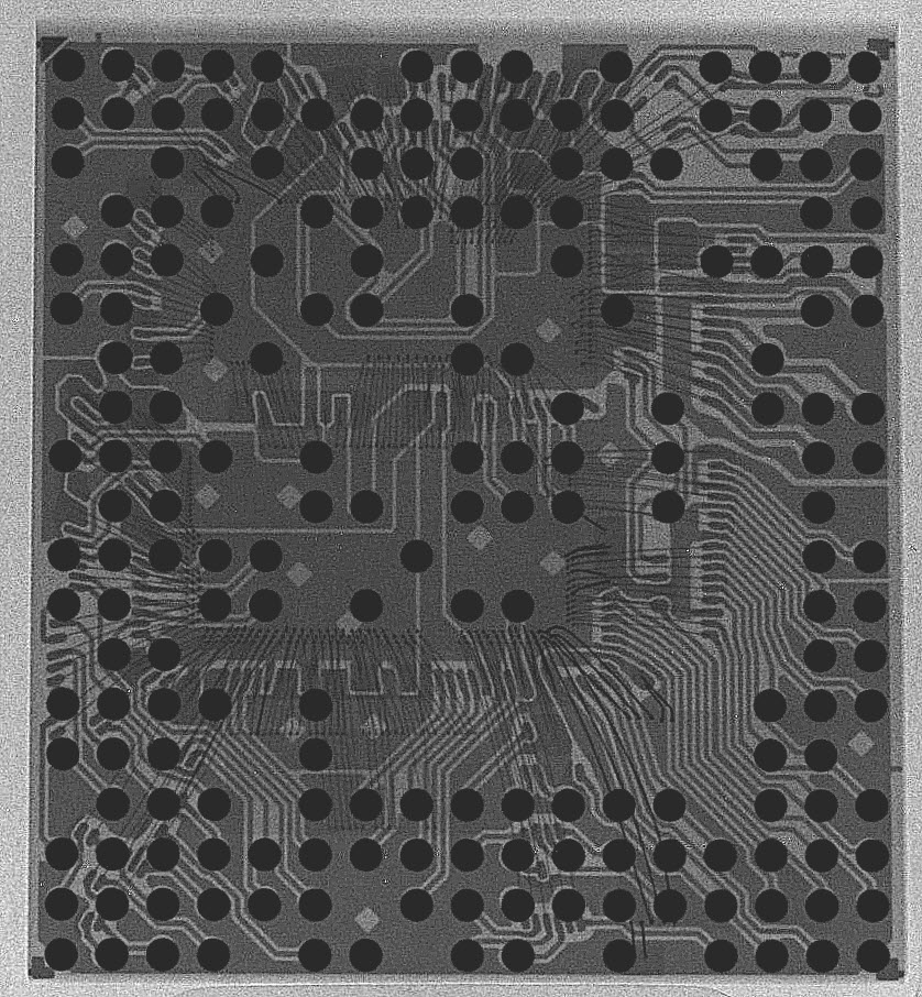
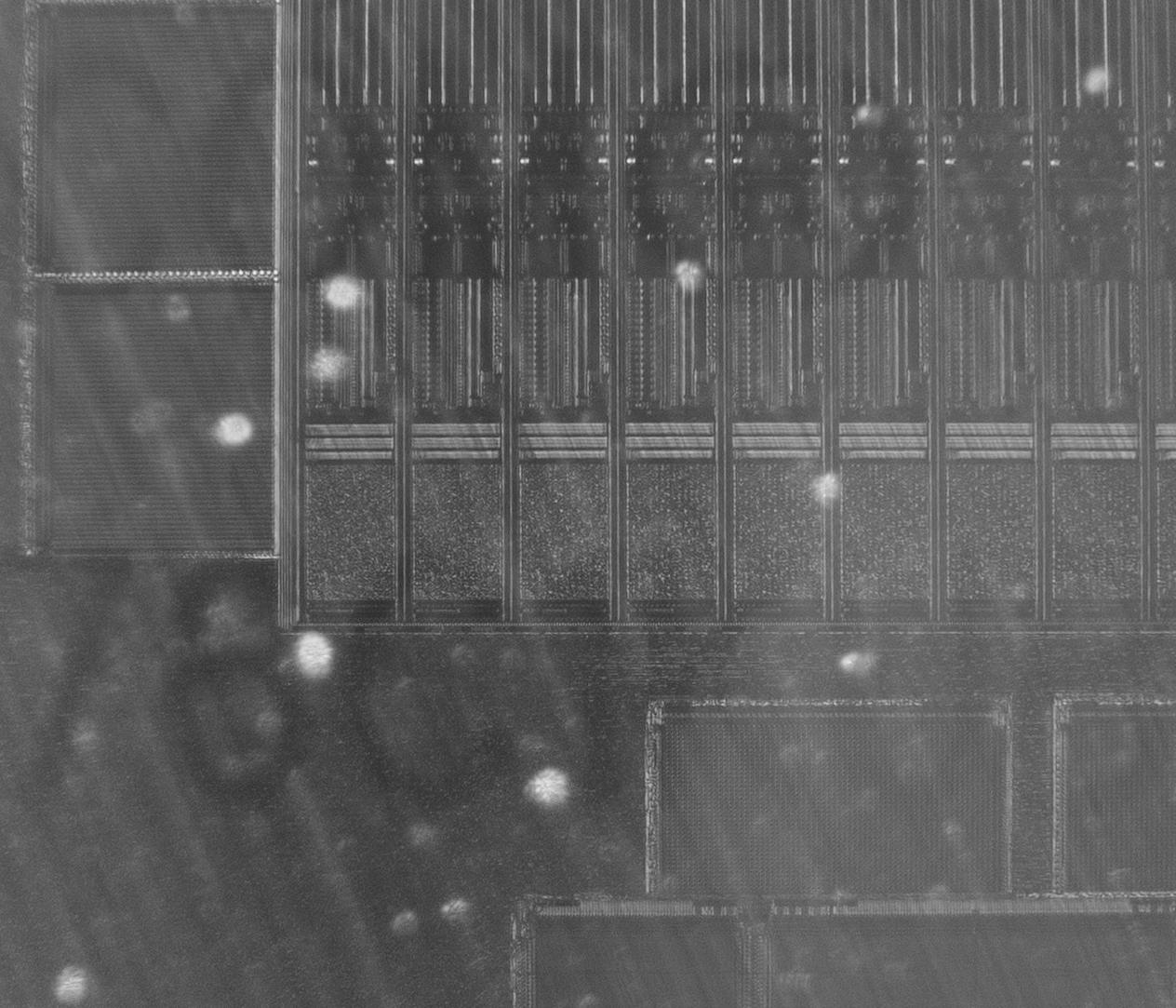
Here’s an example of the MPW7 run on SKY130A, courtesy of Matt Venn, imaged using my automated IRIS machine:

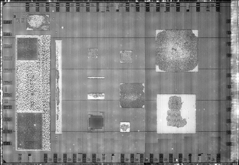
The above is just a thumbnail; click on the image to zoom into and browse the full-resolution version at siliconpr0n.org (and check out my collection on that server for some more full-chip IRIS images). Each of the mottled dots in the lighter-shaded rectangles in the image corresponds to a logic gate, flip flop, or a “fill cell” (dummy transistors wired up as decoupling capacitors). To create the image, I just had to tell the machine where three corners of the chip are, and it automatically focuses and scans the full area. A script then post-processes the tiles into the fully-composed image you see here.

A broad goal of the project is to democratize silicon imaging and improve the state of the art in hardware verification. This is an area where simply popularizing silicon imaging can move the needle on security for everyone, because a credible threat of being caught reduces the incentive for adversaries to invest in expensive Trojan-implantation capabilities.

The good news is that the project is now at a state where, over the next couple of months, I can share a series of posts that detail the methodology used to develop the automated IRIS system, as well as document the construction of the device.

To kick things off, I’m going to start with a review of the current state of the art in hardware verification.

Review: Current State of the Art in Hardware Verification

Is my computer trustworthy? How do I know it was built correctly, and will execute my instructions faithfully? These are the questions that hardware verification aims to answer.

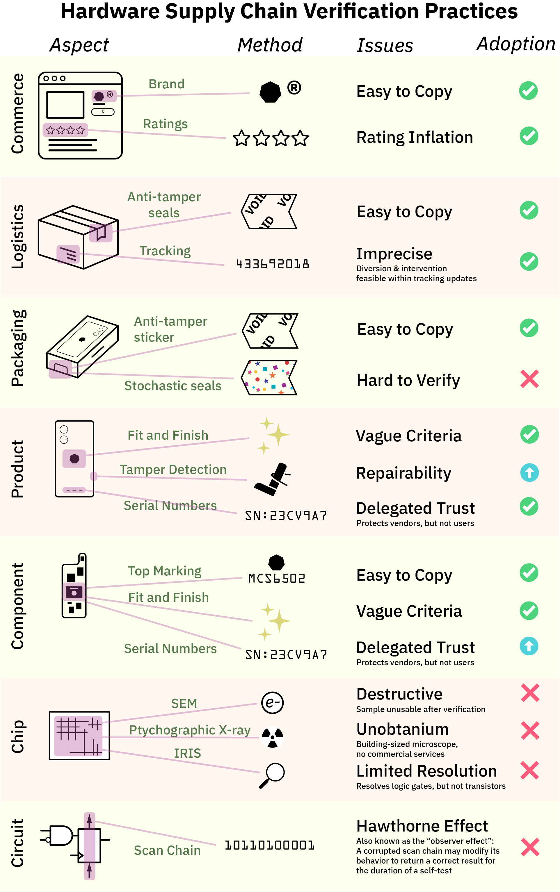
Hardware verification happens at every level of the supply chain. Let’s start with the relatable, every-day problem of how do I pick a piece of hardware to buy, and from there dive all the way down to esoteric topics such as verifying the circuits and devices that make up the hardware itself.

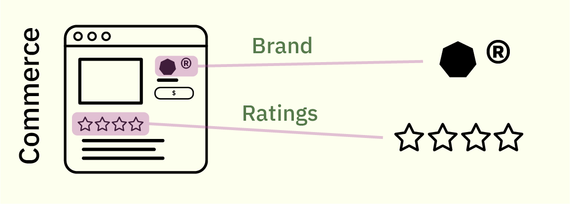
Consumers shopping for a computer rely principally on reputation mechanics to make choices: is the manufacturer a reputable brand? And how do my peers rate it?

Many of us can relate to how these mechanisms can fail. Ratings can be inflated by purchasing fake reviews, and stores can sell counterfeit brand goods. “Surely, this is just a problem of the retail market”, one might think. Once we’ve waded through the swamp of advertisements and on-line storefronts, the powers that be ought to ensure the device we ordered is the device we get! Otherwise it’s like, fraud or something bad like that, right?

Unfortunately, the level of sophistication for verification at every level of the supply chain is precisely as much as it needs to be for the vendor to get away with it, and not one iota more. For example, when it comes to logistics, we largely rely upon anti-tamper seals and tracking numbers to make sure our package arrives intact.

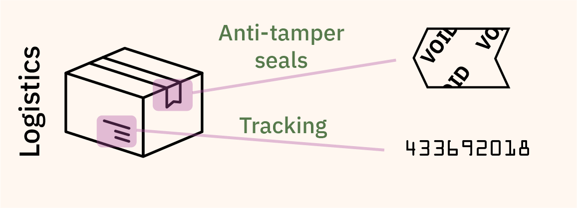
These measures are generally effective at deterring petty theft, but most anti-tamper tape can be purchased by the roll on gray markets, and tracking updates are too infrequent to rule out package diversion and intervention. Besides, that, consumers are conditioned to accept packages that have been mis-routed or experienced an “exception” during delivery – few will return an item that was delivered a day late under fears that the item could have spent a night in a facility where back doors were installed. Our ready acceptance of delivery exceptions is just one example of how supply chains are only as tight as they need to be for broad consumer acceptance, and not one iota more.

Once you’ve received the shipping box, most high-end consumer electronics have additional seals on their packaging. Unfortunately, most seals rely on easy-to-copy anti-tamper solutions such as holograms or fine printing; or at best contain serial numbers that are easy to copy yet have no easy way to check for authenticity.

Solutions such as glitter seals or other stochastic seals that rely upon the randomness inherent in paper fiber or glue to create a unique, unforgeable seal for every package have been proposed, but adoption is low and there is a lack of standardized, easy-to-use verification tools for such seals. Again, packaging seals are just as good as they need to be for broad consumer acceptance, no more, no less.

At the product level, there is a modicum of good news, at least in certain classes of products.

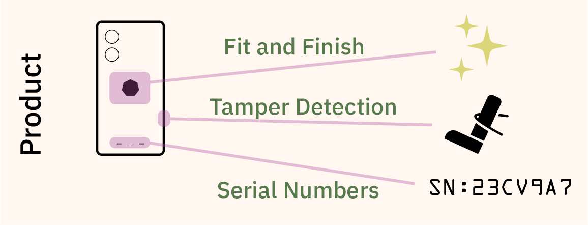
The traditional route of verification – observing the “fit and finish” of a product to detect counterfeits – is still the dominant method for most consumer products. However, in mobile phones and some laptops, manufacturers deploy electronic serial numbers and tamper detection techniques to deter would-be thieves of components or sub-assemblies. The effectiveness of these techniques depend intimately upon the implementation details; but in any case, they incur a cost in repairability and often times the end consumer can’t access the vendor’s databases to check that everything is in order. Instead, consumers are forced to delegate their trust to the vendors; yet regular consumers have no way to audit the vendors. The deferred trust boogeyman haunts everything from Apple’s iPhone ecosystem, to Intel’s SGX remote attestation mechanisms.

One would hope that this increase in verification sophistication is a trend that improves the deeper you go into the underlying technology. Unfortunately, it’s quite the opposite.

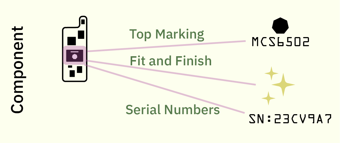
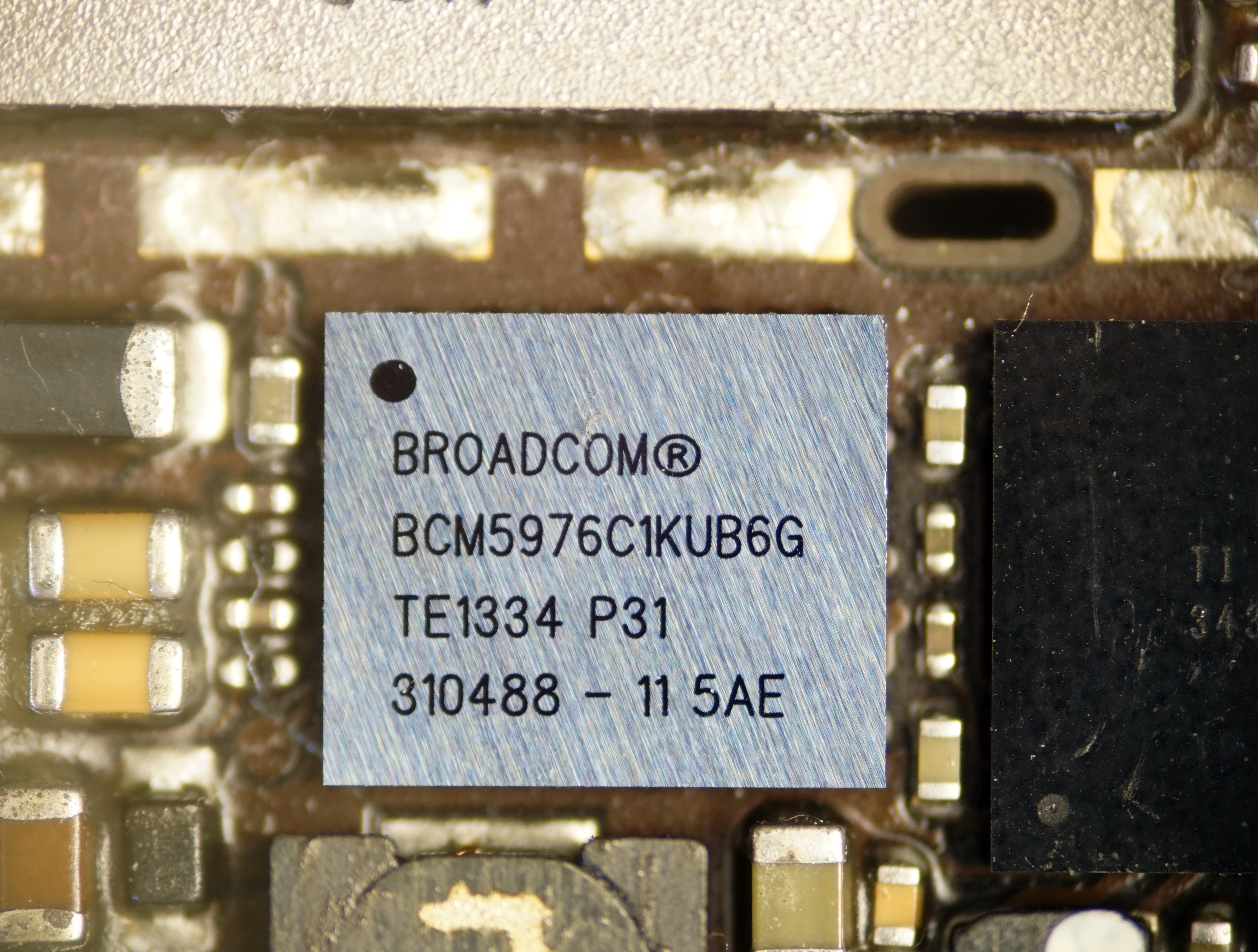
At the component level, the standard to this day for verifying the authenticity of a component is to look at the top marking (that is, the laser-etched numbers and logo) and the fit and finish of the package. Counterfeiters will often miss subtle details such as the font of the numbering, the location of the pin 1 marking, the composition of the overmold material, etc. Factories train staff to inspect and detect defects based on these irregularities.

What happens when a counterfeiter gets all these factors right? Well … the component goes into production, and we find out later about problems, either due to the assemblies failing test in the factory, or perhaps failing in peculiar ways in the field. For better or for worse, these problems are rare, generally affecting less than single-digit percentages of end users, and absent specific requirements or payments from customers to do more, equipment makers do exactly this and nothing more to protect the supply chain.

Even though most modern microcontrollers ship with an electronic serial number, few device manufacturers take advantage of them, and, perhaps somewhat surprisingly, there is usually no easy way to authenticate serial numbers with the component maker. Often times the purpose of the serial number is to serve as a unique ID for tracking products once manufactured; they are not structured to serve as a cryptographic method for determining provenance of the chip itself. Some security-forward microcontrollers feature things like PUFs (physically unclonable functions), but their implementation is usually directed at preventing people from tampering with or servicing their devices, rather than enabling users to verify the construction of the device itself.

And that’s about it – this is where any attempt to verify our electronics stops. To a first order, nobody even looks at the wires inside the chip.

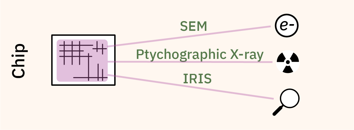
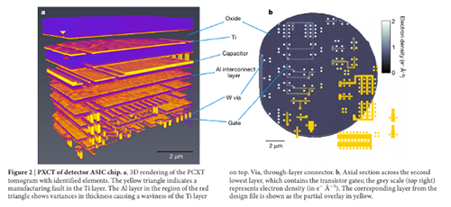
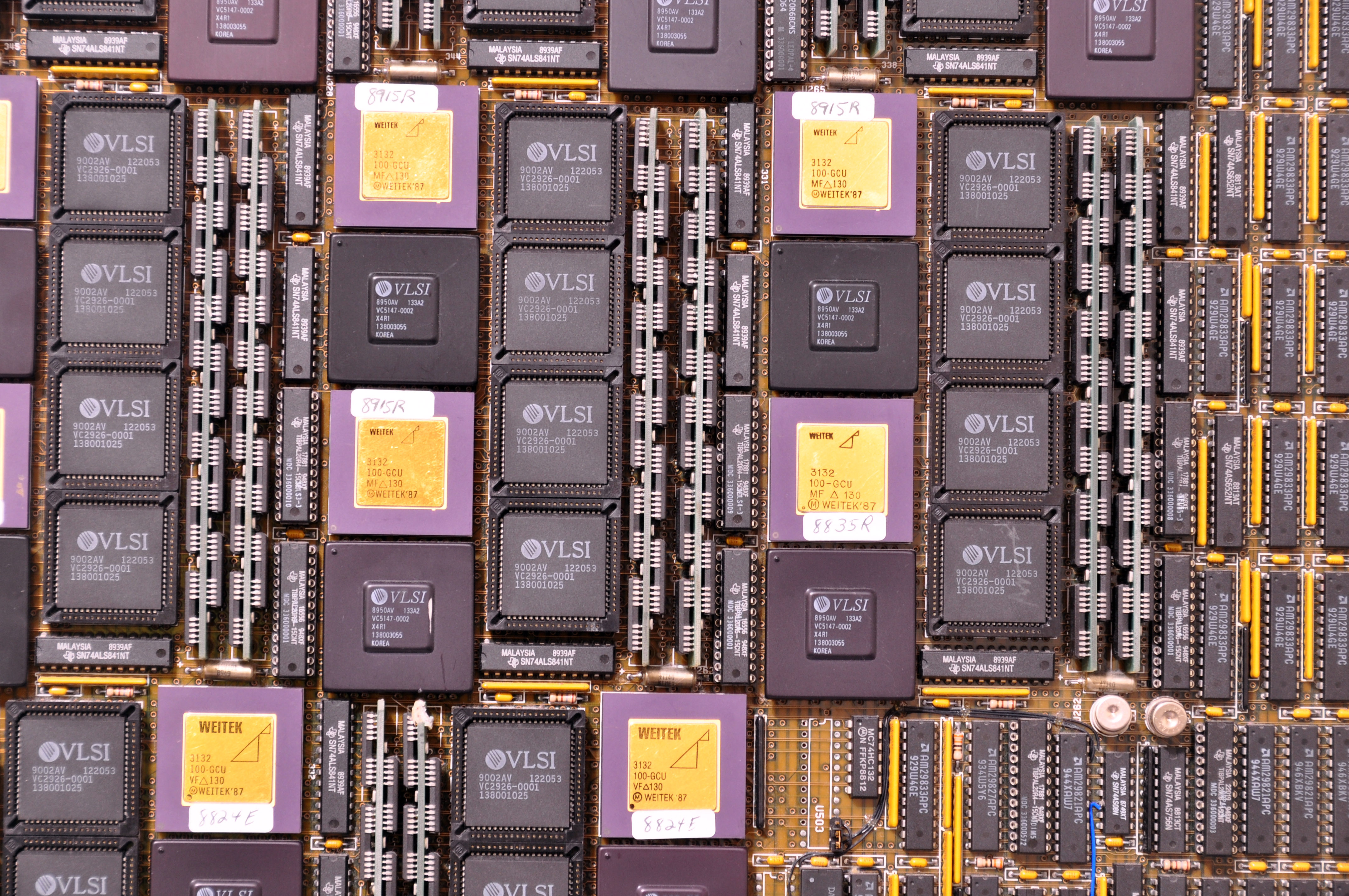
This is because prior to IRIS, your options for inspecting silicon are either destructive, or experiments conducted in high energy physics labs. If you’ve ever seen the brilliant teardowns done by companies like TechInsights, the chips are generally imaged at the circuit level with a SEM or FIB, which requires the chip to be removed from its package and some of the metal layers to be permanently stripped off. Thus, one can obtain extremely high-quality imagery of a sample chip, but these techniques cannot be used to verify the very chip you want to use inside your computer, as the imaged chip must be destroyed.

An alternative, non-destructive technique known as X-ray ptychography can be thought of as a very high resolution 3D scanner for circuits. It’s very impressive, but to date it can only be done in a handful of high energy physics labs and it takes a long time (about three hours for 20 cubic microns) to image a full chip.

The technique I’m developing, IRIS, is a non-destructive technique to acquire micron-resolution images of the first metal layer of a chip at a rate of a seconds per square millimeter. To the best of my knowledge, this is the first practical technique that gives users a glimpse of the actual circuits they will use after it has been mounted on a circuit board.

There’s one final layer deeper into the technology stack beyond imaging of the circuits: electrically testing the circuits directly with a technique known as a “scan chain”. The good news is that scan chains are a mature technology; the bad news is that it is almost never done by users because the details of the scan chain are kept secret, and that a scan chain inspection alone can be easily defeated by a malicious adversary.

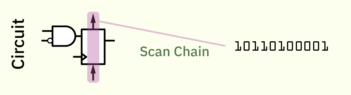
The purpose of a scan chain is to assist with the rapid detection of fabrication defects. It works by adding an extra path to a finished design that strings every register into one or more chains. Bit patterns are loaded into the chain, and the resulting logical operations performed by the gates connected between the registers is observed on the output of the chain. With enough patterns, you can build up an idea of what logic is between every register. Of course, the space of bits to explore grows exponentially with the number of bits in a chain, so it’s not practical to brute-force a large state space.

As a result, scan chains are good for detecting flaws in known circuits introduced by mother nature, but ineffective at deterring a malicious adversary. This is true even if one could brute-force the entire state-space due to the epistemic circularity of trusting a circuit to test itself. More colloquially, one may have heard of the “Hawthorne Effect” or the “observer effect”, which describes a subject under study temporarily altering their behavior because they know they are being studied, thus affecting the results of the study. In this case, a scan chain knows when it’s being queried, and thus, a malicious modification to a scan chain can add hidden states that alter its behavior for the duration of a scan, allowing it to pretend to be correctly constructed, but only when a check is actively running.

Although almost every chip goes through a scan chain test before it is shipped, the test vectors are proprietary, and often times the scan chains are deliberately and permanently sealed in a way to make it impossible for users to access. Scan chains may be scuttled after the factory test for ostensible security reasons, as an adversary can use them to read out the full state of a chip. However, depending on the threat model, it may be preferable to give users the option to exercise the scan chain and then permanently fuse out the scan chain after inspection.

Filling in the Verification Gap

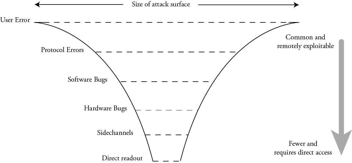
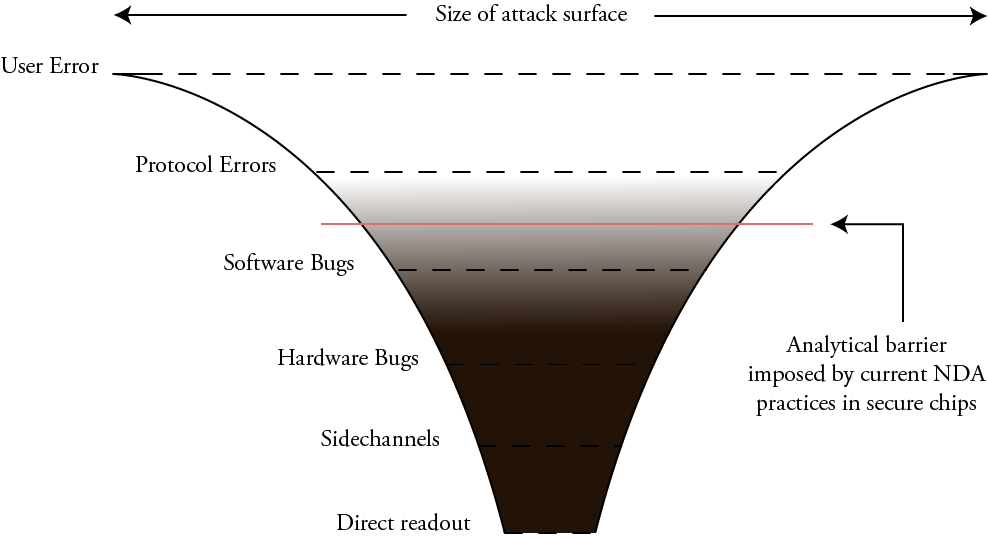
As the summary chart below shows, supply chain verification techniques, although imperfect, enjoy broad adoption at the component level and above. However, there is a significant gap in user verification starting at the chip level and below.

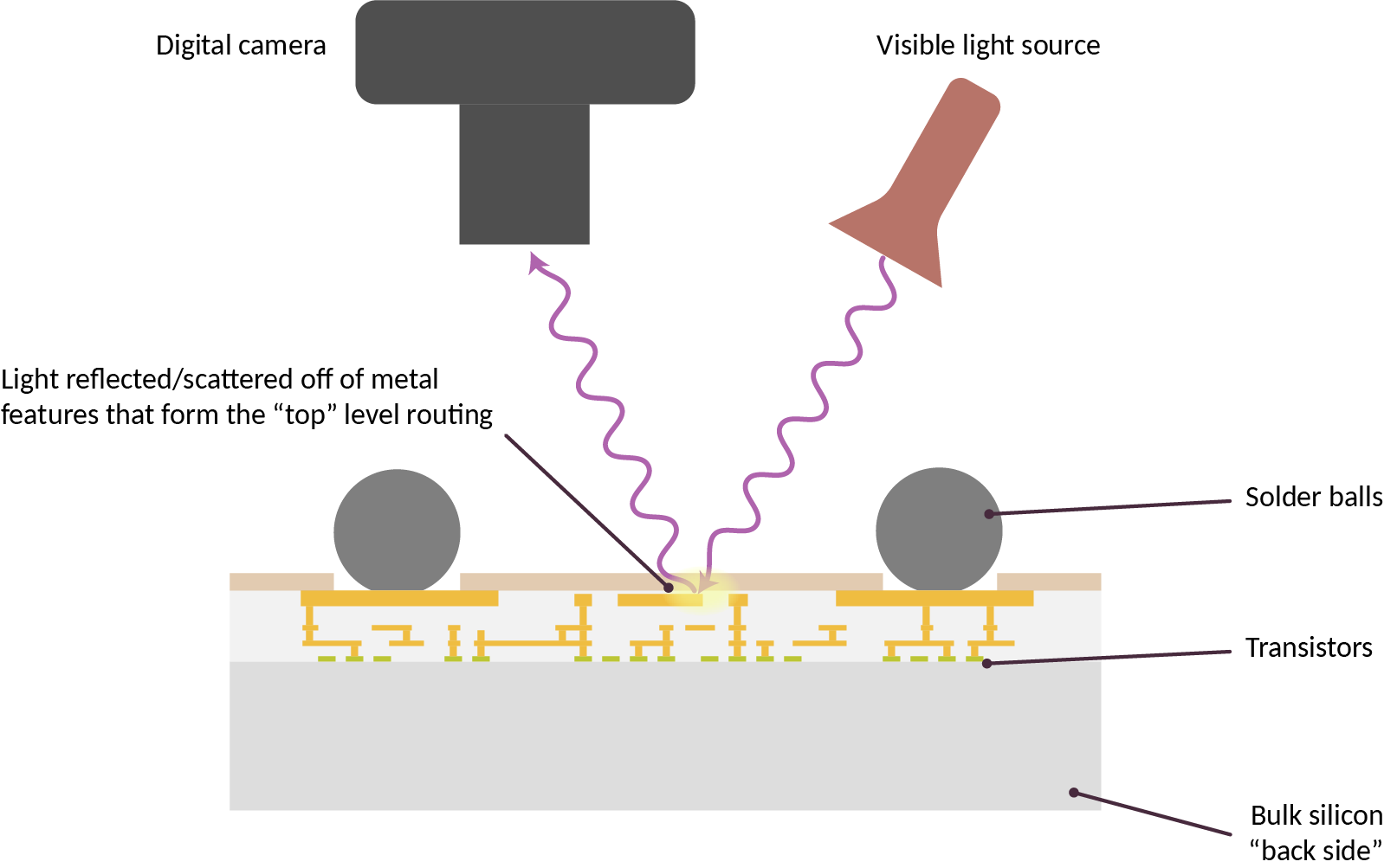
My work, the Infra-Red, in situ (IRIS) inspection of silicon, is a step toward filling in this verification gap. In its simplest form, chips are deliberately constructed for optical inspection with infra-red light shined through the back side of the chip – that is, the side facing “up” that is not bonded to the circuit board.

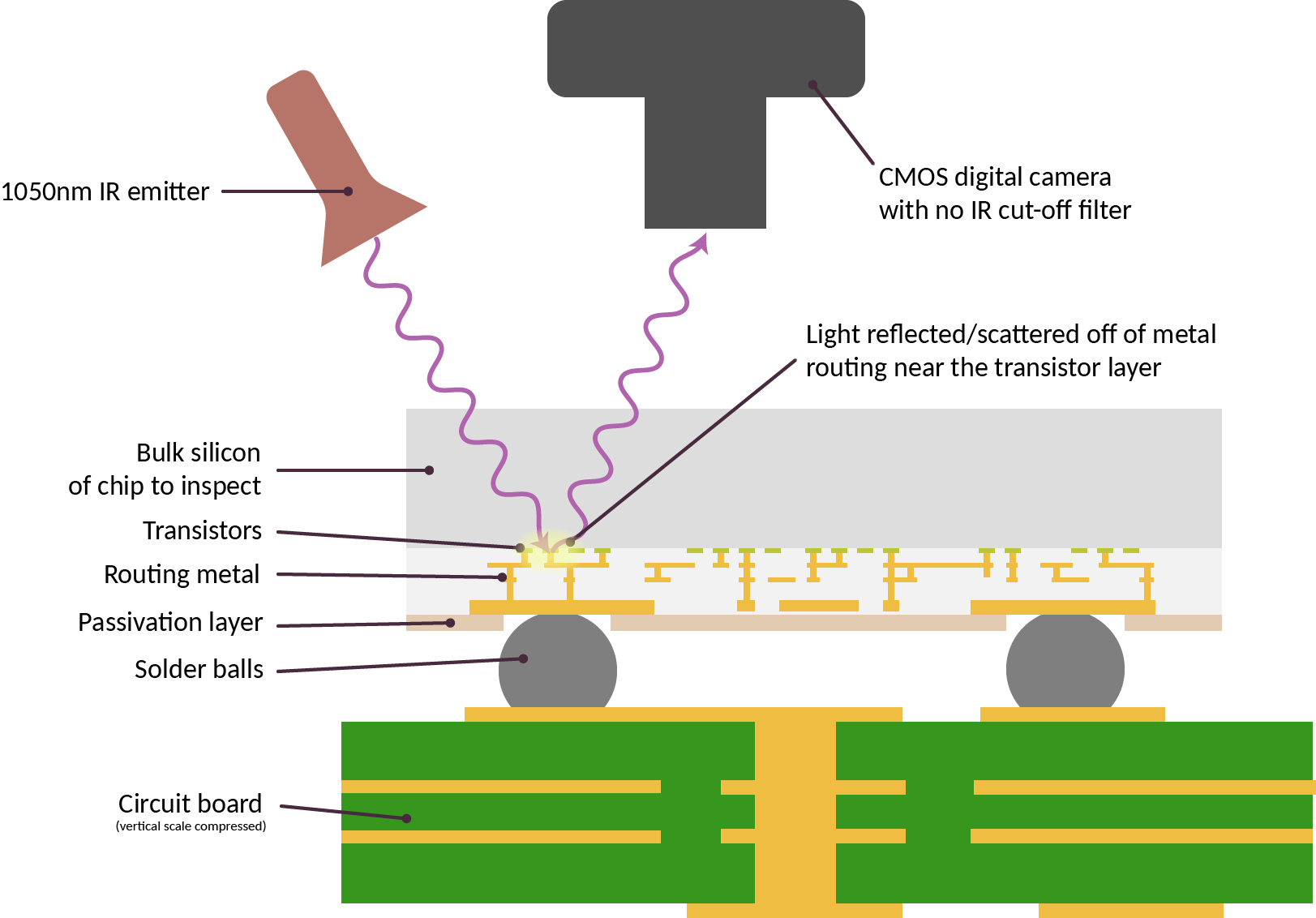
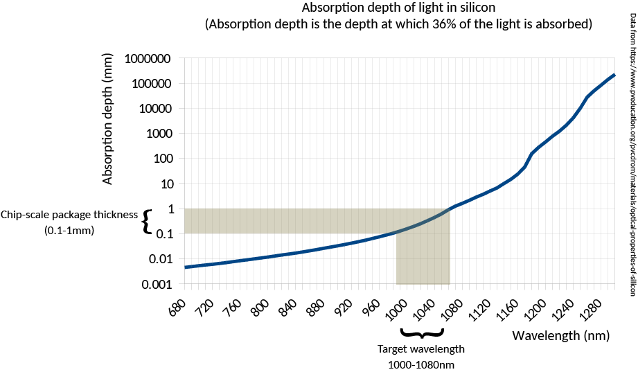
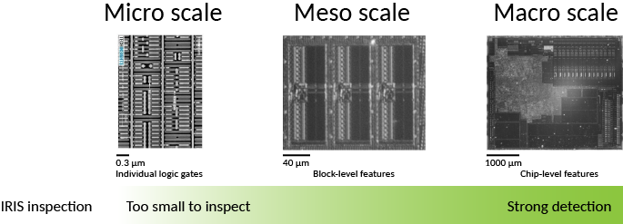
The technique works because although silicon looks opaque at visible light, it is transparent starting at near-infrared wavelengths (roughly 1000 nm and longer). Today’s commodity optics and CMOS cameras are actually capable of working with lights at this wavelength; thus, IRIS is a low-cost and effective technique for confirming the construction of chips down to block level. For example, IRIS can readily help determine if a chip has the correct amount of RAM, number of CPU cores, peripherals, bond pads, etc. This level of verification would be sufficient to deter most counterfeits or substitutions.

However, due to the diffraction limit of infra-red light, it is insufficient for transistor-level imaging. Furthermore, it can only reliably infer the existence of the metal layers closest to the transistors (in technical jargon, it can infer the existence of “standard cell” library elements); it cannot reveal too much information about the higher-level metal wires that route between logic gates.

Thus, for threat models which require protection against adversaries capable of manipulating wires on an integrated circuit, IRIS should be combined with scan chain techniques to robustly verify a chip’s construction.

Hybrid Verification For the Win

As alluded to previously, scan chains alone are insufficient for detecting modifications to a circuit, because an adversary may modify the scan chain in such a manner that it responds with correct answers during the scan itself, but behaves maliciously otherwise.

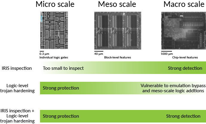
However, such modifications require the introduction of additional logic gates to track the scan state and compute both correct and malicious responses. Because IRIS can “see” logic gates, it is able to put a firm upper bound on the potential amount of additional logic present in an integrated circuit. Thus, the combination of IRIS and scan chain techniques may be able to effectively verify that a circuit is correctly constructed.

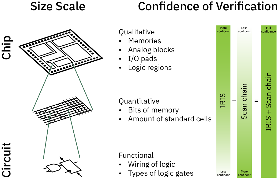
The diagram above illustrates how IRIS and scan chain techniques compliment each other to obtain a high-confidence verification of a chip’s structure.

  • At the largest scales, IRIS can trivially quantify the number of IP blocks, pads, analog functions and memories; this is in contrast to scan-chain techniques which may struggle to characterize analog functions and other macro-scale properties, due to factors such as the analog limitations of scan chains, and the exponential growth of state-space to explore at the macro-level.
  • At intermediate scales, IRIS can quantify the number of bits of memory, or bound the number of standard cells in a region. This places constraints on how much malicious logic could be injected that could otherwise defeat a scan chain test.
  • At the smallest scales, IRIS cannot discern individual wires or gates. However, scan chain excels at exploring the topology and function of logic at the smallest and most local increments.

Thus, in combination, the two techniques may be used to achieve a high confidence verification of a chip’s function – at a cost and time scale suitable for point-of-use (e.g. end user) verification. I say “high confidence” because in the end, there is a probabilistic nature to both imaging and scan chain pattern coverage. As future work I’d like to explore the possibility of using formal methods to mathematically rule out any escapes, but absent formal proofs, it is important to understand that the technique is probabilistic in nature. That being said, it is still vastly better than the current state of the art, which is doing nothing at all.

Hybrid verification could be a viable path toward filling in the verification gap at the most fundamental levels of the supply chain, assuming chip vendors are willing to facilitate such verification by designing and packaging their products in a manner conducive to optical verification, and assuming chip vendors are willing to share scan chain test vectors with end users.

IRIS: Where We Are, and Where We are Headed

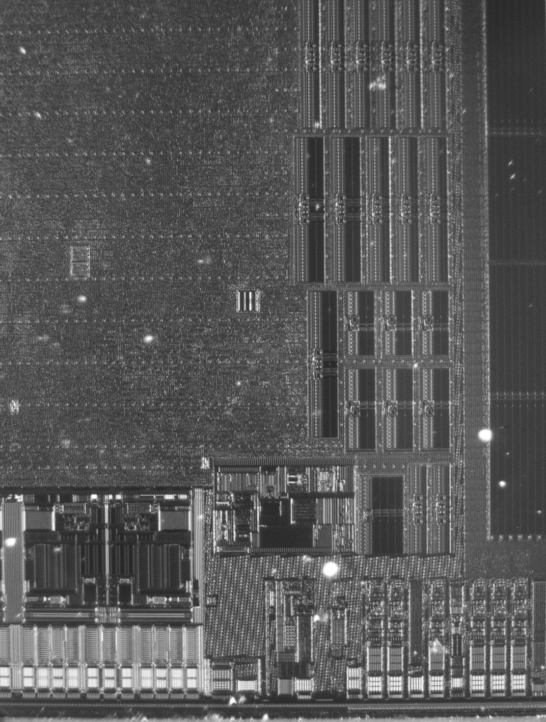
Because of the 1000 nm wavelength limit imposed by the transparency of silicon, IRIS has a limit on the features it can resolve. Below is an example IRIS imaging a small part of a RISC-V core on a 130nm chip fabricated using the SKY130A open PDK from Matt Venn’s MPW7 run; you can browse the entire chip image here.

Use the slider to compare the base image against an overlay derived from the design files. Each colored rectangle in the overlay corresponds to a “standard cell”: blue are flip flops, pink are filler/capacitor cells, aqua are varieties of and-or-invert gates, etc. Note that the native resolution of the image above is 1469 pixels wide; it has been scaled down to fit the width of this page.

One can see that in a 130nm process, IRIS has a reasonable chance of conducting a gate-count census of an entire chip. And yes, it’s not atypical for chips to be limited not by logic density, but by wiring density; hence, the majority of a chip’s active area contains filler cells (the pink rectangles).

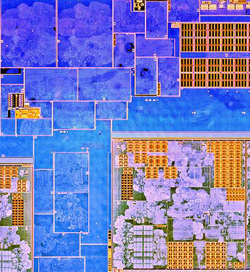
Above is of an identically scaled region of a 22nm chip, again of a RISC-V core, but this time almost the entire core is within view because the logic gates are, unsurprisingly, much smaller: a single gate can be as small as a few pixels. At this node, IRIS can place an upper bound on gate count to within a couple dozen extra flip flops.

An important caveat when comparing images above: the backside finish of the 130nm chip is a mirror polish, but the 22nm chip only went through backgrinding; in other words, the 22nm chip’s image clarity is degraded due to a series of small surface ridges that refract light. If the 22nm chip had the same mirror-finish quality as the 130nm chip, the imaging resolution of the 22nm chip would be improved. Back side polishing of chips is not a difficult or uncommon process, but it’s not done unless explicitly required. Thus, chips intended for optical verification should specify a high quality mirror finish for the back side.

IRIS goes hand-in-hand with electrical scan chains to achieve full chip verification. Scan chains are able to quickly confirm the wiring between small clusters of standard cells, but Trojans can evade detection by including an honest copy of the affected logic. IRIS confirms that a given cluster of logic being tested by a scan chain is approximately the right size. The search perimeter for rouge cells is reduced by running the scan chain test at high speeds. Ideally, the total bounds are tight enough to rule out the existence of sufficient extra logic to evade detection in scan chain testing.

In other words, what IRIS can’t directly image, the scan chain has to make up for with complexity of test. Thus, at 130nm, a simple bit-shift scan chain may be sufficient, since individual gates are resolvable; at 22nm, a more complicated technique splitting the scan chain into multiple segments, capable of challenging the system with mutually unpredictable data patterns, may be required to drive up the lower bound on circuit complexity to the “dozens of logic gates” range required to bypass the test. And at the most advanced nodes, even more scan chain segments may be required along with supplementary design techniques to drive the lower confidence bound into the “hundreds of logic gates” range for reliable Trojan detection with IRIS.

In general, when I use the term “IRIS” alone in a context where high-confidence gate level verification is required, readers should infer that I’m referring to some kind of hybrid verification technique of both IRIS and scan chain.

That being said, I envision IRIS mainly being used to verify high-value circuitry, such as those found in a discrete cryptographic enclave intended to store secrets such as root keys. These enclaves would not require the performance or density of the latest process nodes. With careful design, a 22nm or 28nm process can offer GHz clock speeds, sufficient for storing and processing bulk data with root secrets. The “2x” nm node is particularly interesting because it is the best “value per transistor” sweet-spot, and likely to stay that way for the foreseeable future: it’s the smallest process node that still uses the easier-to-fabricate planar CMOS transistors while requiring only single-patterning DUV lithography techniques.

Thus, the bulk of my on-going research will focus on samples produced in 130nm and 180nm (because there are Open PDKs available for those nodes today), and 22nm (because of the ultimate economic importance of the node). I am also betting that while the 2x nm node is not open source today, it will become more open within the next decade if the world continues on a “business as usual” scenario where technology continues to race down the commodification curve, and fabs continue to compete on price and need more designs to keep them busy and profitable.

While the imaging system has met its initial goals, the software still has miles to go before I sleep (And miles to go before I sleep). In particular, I’m still working on training a computer to automatically recognize patterns of gates in IRIS images and to generate a gate count census. I’d also ideally like to find a way to use formal methods to place an upper bound on the amount of logic one can hide in a scan chain for a given testing methodology, so designers can have a formally proven tool to validate that their scan chains are sufficiently dense so that IRIS can pick up any attempts to bypass them. Unfortunately, I’m neither a software engineer nor a mathematician, but the problems are interesting enough that I’ll still give them a go. Worst case, I will learn something new along the path to failure.

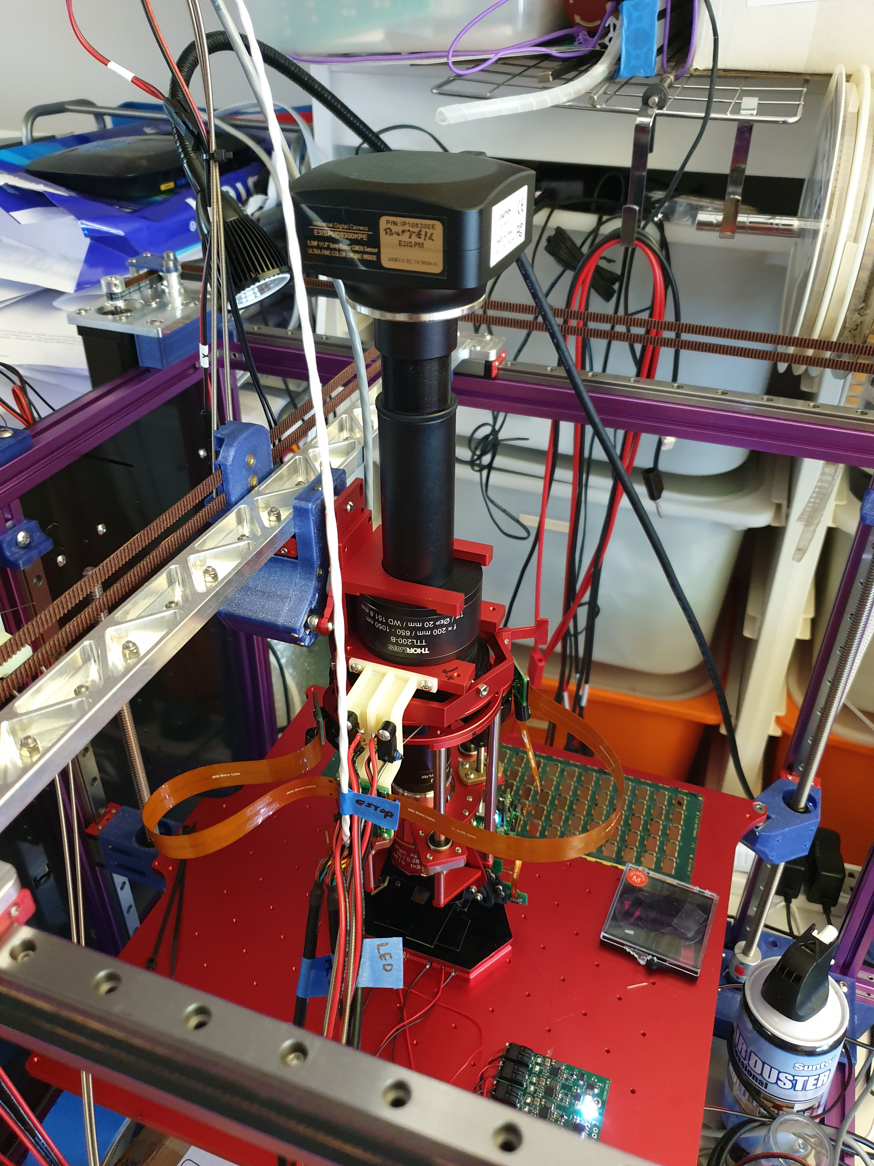
Above is the IRIS machine that I’ve built. There’s a lot going on here – but basically, it’s an IR camera attached to a microscope, a nanometer-resolution focusing mechanism, and a pair of 1050nm light sources that have continuously adjustable azimuth and zenith. This microscope assembly is mounted in a Jubilee motion platform. The Jubilee is open source, and was designed by Sonya Vasquez of Prof. Nadya Peek‘s Machine Agency group. I got it as a kit from Filastruder. The base motion platform is capable of 10 micron steps, and features a kinematically coupled Z-bed with three independent actuators, allowing me to dynamically compensate for planarity issues in the sample undergoing imaging.

Above is a short video loop showing the core mechanics in action. The weird thing on the bottom with the red and black wires coming out of it is the kinematically coupled nanometer-resolution fine focus stage; its motions are too small to be picked up by the camera.

An explicit goal of this project is to open source all of IRIS, so that anyone can replicate the imaging system. Democratizing chip verification is important because a credible threat of being caught reduces the incentive of adversaries to deploy expensive Trojan-implantation capabilities.

With little fear of being caught, there’s a payoff even if an adversary has to plow tens of millions of dollars into a capability for planting chip-level hardware Trojans in high-value targets. However, if chip inspection equipment can purchased in the ballpark of hundreds to perhaps thousands of dollars, and more than a handful of users are known to routinely inspect chips, the path to payoff for an adversary before they are caught becomes murky. In this case, a rational adversary may be deterred from targeting an IRIS-enabled design, instead reserving their capabilities only for the chips that are difficult to inspect.

Aside from that, I’ll be straight with you – a big motivation for IRIS is simply because I am curious, and I want to look inside chips and see how they are built (and it’s kind of fun and strangely satisfying to build robots). I haven’t been disappointed with what I’ve seen so far – I have to stop myself from wasting evenings browsing through the construction of chips. I’ve done a bit of chip design in the past, and it’s fascinating to see the diversity of techniques and new trends in chip designs. I’m excited to share this sense of wonder with kindred spirits!

Given the volume of material to cover, I’m going to break the documentation up into a series of blog posts that go into the methodology used to build the machine, as well as details about every custom component, and the design decisions that went into them. I’ll also summarize the status of the analysis software that accompanies the system – so stay tuned for more posts!

However, if you’re impatient and don’t want to wait for the documentation, you can already browse the source files for the microscope, control software, stitching software, and layout extraction software.

Finally, a big shout-out to NLnet and the European Commission. NLnet’s NGI0 Entrust fund, established with support from the European Commission’s Next Generation Internet Program, are instrumental in facilitating my work on IRIS. Also a big shout-out to my Github Sponsors for their incredible generosity and monthly support. Thanks to all these donors, I’m able to keep IRIS 100% open source and free of conflicts of interest with commercial investors.

❤️ Sponsor me on Github! ❤️

Infra-Red, In Situ (IRIS) Inspection of Silicon

Wednesday, March 8th, 2023

Cryptography tells us how to make a chain of trust rooted in special-purpose chips known as secure elements. But how do we come to trust our secure elements? I have been searching for solutions to this thorny supply chain problem. Ideally, one can directly inspect the construction of a chip, but any viable inspection method must verify the construction of silicon chips after they have been integrated into finished products, without having to unmount or destroy the chips (“in situ“). The method should also ideally be cheap and simple enough for end users to access.

This post introduces a technique I call “Infra-Red, In Situ” (IRIS) inspection. It is founded on two insights: first, that silicon is transparent to infra-red light; second, that a digital camera can be modified to “see” in infra-red, thus effectively “seeing through” silicon chips. We can use these insights to inspect an increasingly popular family of chip packages known as Wafer Level Chip Scale Packages (WLCSPs) by shining infrared light through the back side of the package and detecting reflections from the lowest layers of metal using a digital camera. This technique works even after the chip has been assembled into a finished product. However, the resolution of the imaging method is limited to micron-scale features.

This post will start by briefly reviewing why silicon inspection is important, as well as some current methods for inspecting silicon. Then, I will go into the IRIS inspection method, giving background on the theory of operation while disclosing methods and initial results. Finally, I’ll contextualize the technique and discuss methods for closing the gap between micron-scale feature inspection and the nanometer-scale features found in today’s chip fabrication technology.

DOI: 10.48550/arXiv.2303.07406

Side Note on Trust Models

Many assume the point of trustable hardware is so that a third party can control what you do with your computer – like the secure enclave in an iPhone or a TPM in a PC. In this model, users delegate trust to vendors, and vendors do not trust users with key material: anti-tamper measures take priority over inspectability.

Readers who make this assumption would be confused by a trust method that involves open source and user inspections. To be clear, the threat model in this post assumes no third parties can be trusted, especially not the vendors. The IRIS method is for users who want to be empowered to manage their own key material. I acknowledge this is an increasingly minority position.

Why Inspect Chips?

The problem boils down to chips being literal black boxes with nothing but the label on the outside to identify them.

For example, above is a study I performed surveying the construction of microSD cards in an effort to trace down the root cause of a failed lot of products. Although every microSD card ostensibly advertised the same product and brand (Kingston 2GB), a decap study (where the exterior black epoxy is dissolved using a strong acid revealing the internal chips while destroying the card) revealed a great diversity in internal construction and suspected ghost runs. The take-away is that labels can’t be trusted; if you have a high-trust situation, something more is needed to establish a device’s internal construction than the exterior markings on a chip’s package.

What Are Some Existing Options for Inspecting Chips?

There are many options for inspecting the construction of chips; however, all of them suffer from a “Time Of Check versus Time Of Use” (TOCTOU) problem. In other words, none of these techniques are in situ. They must be performed either on samples of chips that are merely representative of the exact device in your possession, or they must be done at remote facilities such that the sample passes through many stranger’s hands before returning to your possession.

Scanning Electron Microscopy (SEM), exemplified above, is a popular method for inspecting chips (image credit: tmbinc). The technique can produce highly detailed images of even the latest nanometer-scale transistors. However, the technique is destructive: it can only probe the surface of a material. In order to image transistors one has to remove (through etching or polishing) the overlying layers of metal. Thus, the technique is not suitable for in situ inspection.

X-rays, exemplified in the above image of a MTK6260DA , are capable of non-destructive in situ inspection; anyone who has traveled by air is familiar with the applicability of X-rays to detect foreign objects inside locked suitcases. However, silicon is nearly transparent to the types of X-rays used in security checkpoints, making it less suitable for establishing the contents of a chip package. It can identify the size of a die and the position of bond wires, but it can’t establish much about the pattern of transistors on a die.

X-Ray Ptychography is a technique using high energy X-rays that can non-destructively establish the pattern of transistors on a chip. The image above is an example of a high-resolution 3D image generated by the technique, as disclosed in this Nature paper.

It is a very powerful technique, but unfortunately it requires a light source the size of a building, such as the Swiss Light Source (SLS) (donut-shaped building in the image above), of which there are few in the world. While it is a powerful method, it is impractical for inspecting every end user device. It also suffers from the TOCTOU problem in that your sample has to be mailed to the SLS and then mailed back to you. So, unless you hand-carried the sample to and from the SLS, your device is now additionally subject to “evil courier” attacks.

Optical microscopy – with a simple benchtop microscope, similar to those found in grade-school classrooms around the world – is also a noteworthy tool for inspecting chips that is easier to access than the SLS. Visible light can be a useful tool for checking the construction of a chip, if the chip itself has not been obscured with an opaque, over-molded plastic shell.

Fortunately, in the world of chip packaging, it has become increasingly popular to package chips with no overmolded plastic. The downside of exposing delicate silicon chips to possible mechanical abuse is offset by improved thermal performance, better electrical characteristics, smaller footprints, as well as typically lower costs when compared to overmolding. Because of its compelling advantages this style of packaging is ubiquitous in mobile devices. A common form of this package is known as the “Wafer Level Chip Scale Package” (WLCSP), and it can be optically inspected prior to assembly.

Above is an example of such a package viewed with an optical microscope, prior to attachment to a circuit board. In this image, the back side of the wafer is facing away from us, and the front side is dotted with 12 large silvery circles that are solder balls. The spacing of these solder balls is just 0.5mm – this chip would easily fit on your pinky nail.

The imaged chip is laying on its back, with the camera and light source reflecting light off of the top level routing features of the chip, as illustrated in the cross-section diagram above. Oftentimes these top level metal features take the form of a regular waffle-like grid. This grid of metal distributes power for the underlying logic, obscuring it from direct optical inspection.

Note that the terms “front” and “back” are taken from the perspective of the chip’s designer; thus, once the solder balls are attached to the circuit board, the “front side” with all the circuitry is obscured, and the plain silvery or sometimes paint-coated “back side” is what’s visible.

As a result, these chip packages look like opaque silvery squares, as demonstrated in the image above. Therefore front-side optical microscopy is not suitable for in situ inspection, as the chip must be removed from the board in order to see the interesting bits on the front side of the chip.

The IRIS Inspection Method

The Infra-Red, In Situ (IRIS) inspection method is capable of seeing through a chip already attached to a circuit board, and non-destructively imaging the construction of a chip’s logic.

Here’s a GIF that shows what it means in practice:

We start with an image of a WLCSP chip in visible light, assembled to a finished PCB (in this case, an iPhone motherboard). The scene is then flooded with 1070 nm infrared light, causing it to take on a purplish hue. I then turn off the visible light, leaving only the infrared light on. The internal structure of the chip comes into focus as we adjust the lens. Finally, the IR illuminator is moved around to show how the chip’s internal metal layers glint with light reflected through the body of the silicon.

Here is a still image of the above chip imaged in infra-red, at a higher resolution:

The chip is the BCM5976, a capacitive touchscreen driver for older models of iPhones. The image reveals the macro-scopic structure of the chip, with multiple channels of data converters on the top right and right edge, along with several arrays of non-volatile memory and RAM along the lower half. From the top left extending to the center is a sea of standard cell logic, which has a “texture” based on the routing density of the metal layers. Remember, we’re looking through the backside of the chip, so the metal layer we’re seeing is mostly M1 (the metal connecting directly to the transistors). The diagonal artifacts apparent through the standard cell region are due to a slight surface texture left over from wafer processing.

Below is the region in the pink rectangle at a higher magnification (click on the image to open a full-resolution version):

The magnified region demonstrates the imaging of meso-scopic structures, such as the row and structure column of memory macros and details of the data converters.

The larger image is 2330 pixels wide, while the chip is 3.9 mm wide: so each pixel corresponds to about 1.67 micron. To put that in perspective, if the chip were fabricated in 28 nm that would correspond to a “9-track” standard cell logic gate being 0.8 microns tall (based on data from Wikichip). Thus while these images cannot precisely resolve individual logic gates, the overall brightness of a region will bear a correlation to the type and density of logic gate used. Also please remember that IRIS is still at the “proof of concept” stage, and there are many things I’m working on to improve the image quality and fidelity.

Here’s another demo of the technique in action, on a different iPhone motherboard:

How Does It Work?

Silicon goes from opaque to transparent in the range of 1000 nm to 1100 nm (shaded band in the illustration below). Above 1100 nm, it’s as transparent as a pane of glass; below 1000 nm, it rapidly becomes more opaque than the darkest sunglasses.

Meanwhile, silicon-based image sensors retain some sensitivity in the near-to-short wave IR bands, as illustrated below.

Between these two curves, there is a “sweet spot” where standard CMOS sensors retain some sensitivity to short-wave infrared, yet silicon is transparent enough that sufficient light passes through the layer of bulk silicon that forms the back side of a WLCSP package to do reflected-light imaging. More concretely, at 1000 nm a CMOS sensor might have 0.1x its peak sensitivity, and a 0.3 mm thick piece of silicon may pass about 10% of the incident light – so overall we are talking about a ~100x reduction in signal intensity compared to visible light operations. While this reduction is non-trivial, it is surmountable with a combination of a more intense light source and a longer exposure time (on the order of several seconds).

Above is a cross-section schematic of the IRIS inspection setup. Here, the sample for inspection is already attached to a circuit board and we are shining light through the back side of the silicon chip. The light reflects off of the layers of metal closest to the transistors, and is imaged using a camera. Conceptually, it is fairly straightforward once aware of the “sweet spot” in infrared.

Two things need to be prepared for the IRIS imaging technique. First, the “IR cut-off filter” has to be removed from a digital camera. Normally, the additional infrared sensitivity of CMOS sensors is considered to be problematic, as it introduces color fidelity artifacts. Because of this excess sensitivity, all consumer digital cameras ship with a special filter installed that blocks any incoming IR light. Removing this filter can range from trivial to very complicated, depending on the make of the camera.

Second, we need a source of IR light. Incandescent bulbs and natural sunlight contain plenty of IR light, but the current demonstration setup uses a pair of 1070 nm, 100 mA IF LED emitters from Martech, connected to a simple variable current power supply (in practice any LED around 1050nm +/- 30nm seems to work fairly well).

To give credit where it’s due, the spark for IRIS came from a series of papers referred to me by Dmitry Nedospadov during a chance meeting at CCC. One published example is “Key Extraction Using Thermal Laser Stimulation” by Lohrke et al, published in IACR Transactions on Cryptographic Hardware and Embedded Systems (DOI:10.13154/tches.v2018.i3.573-595). In this paper, a Phemos-1000 system by Hamamatsu (a roughly million dollar tool) uses a scanning laser to do optical backside imaging of an FPGA in a flip-chip package. More recently, I discovered a photo feed by Fritzchens Fritz demonstrating a similar technique, but using a much cheaper off-the-shelf Sony NEX-5T. Since then, I have been copying these ideas and improving upon them for practical application in supply chain/chip verification.

How Can I Try It Out?

While “off the shelf” solutions like the Phemos-1000 from Hamamatsu can produce high-resolution backside images of chips, the six or seven-figure price tag puts it out of reach of most practical applications. I have been researching ways to scale this cost down to something more accessible to end-users.

In the video below, I demonstrate how to modify an entry-level digital inspection camera, purchasable for about $180, to perform IRIS inspections. The modification is fairly straightforward and takes just a few minutes. The result is an inspection system that is capable of performing, at the very least, block-level verification of a chip’s construction.

For those interested in trying this out, this is the $180 camera and lens combo from Hayear (link contains affiliate code) used in the video. If you don’t already have a stand for mounting and focusing the camera, this one is pricey, but solid. You’ll also need some IR LEDs like this one to illuminate the sample. I have found that most LEDs with a 1050-1070 nm center wavelength works fairly well. Shorter wavelength LEDs are cheaper, but the incidentally reflected light off the chip’s outer surface tends to swamp the light reflected by internal metal layers; longer than 1100 nm, and the camera efficiency drops off too much and the image is too faint and noisy.

Of course, you can get higher quality images if you spend more money on better optics and a better camera. Most of the images shown in this post were taken with a Sony A6000 camera that was pre-modified by Kolari Vision. If you have a spare camera body laying around it is possible to DIY the IR cut-off filter removal; YouTube has several videos showing how.

The modified camera was matched with either the optics of the previously-linked Hayear inspection scope, or directly attached to a compound microscope via a C-mount to E-mount adapter.

Another Sample Image

I’ve been using an old Armada610 chip I had laying around for testing the setup. It’s ideal for testing because I know the node it was fabbed in (55 nm) and the package is a bare flip-chip BGA. FCBGA is a reasonably common package type, but more importantly for IRIS, the silicon is pre-thinned and mirror-polished. This is done to improve thermal performance, but it also makes for very clean backside images.

Above is what the chip looks like in visible light.

And here’s the same chip, except in IR. The light source is shining from the top right, and already you can see some of the detail within the chip. Note: the die is 8mm wide.

Above is the lower part of the chip, taken at a higher magnification. Here we can start to clearly make out the shapes of memory macros, I/O drivers, and regions of differing routing density in the standard cell logic. The die is about 4290 pixels across in this image, or about 1.86 microns per pixel.

And finally, above is the boxed region in the previous image, but a higher magnification (you can click on any of the images for a full-resolution version). Here we can make out the individual transistors used in I/O pads, sense amps on the RAM macros, and the texture of the standard cell logic. The resolution of this photo is roughly 1.13 microns per pixel – around the limit of what could be resolved with the 1070 nm light source – and a hypothetical “9-track” standard cell logic gate might be a little over a pixel tall by a couple pixels wide, on average.

Discussion

IRIS inspection reveals the internal structure of a silicon chip. IRIS can do this in situ (after the chip has been assembled into a product), and in a non-destructive manner. However, the technique can only inspect chips that have been packaged with the back side of the silicon exposed. Fortunately, a fairly broad and popular range of packages such as WLCSP and FCBGA already expose the back side of chips.

Above: Various size scales found on a chip, in relationship to IRIS capabilities.

IRIS cannot inspect the smallest features of a chip. The diagram above illustrates the various size scales found on a chip and relates it to the capabilities of IRIS. The three general feature ranges are prefixed with micro-, meso-, and macro-. On the left hand side, “micro-scale” features such as individual logic gates will be smaller than a micron tall. These are not resolvable with infra-red wavelengths and as such not directly inspectable via IRIS, so the representative image was created using SEM. The imaged region contains about 8 individual logic gates.

In the middle, we can see that “meso-scale” features can be constrained in size and identity. The representative image, taken with IRIS, shows three RAM “hard macros” in a 55 nm process. Individual row sense amplifiers are resolvable in this image. Even in a more modern sub-10 nm process, we can constrain a RAM’s size to plus/minus a few rows or columns.

On the right, “macro-scale” features are clearly enumerable. The number and count of major functional blocks such as I/O pads, data converters, oscillators, RAM, FLASH, and ROM blocks are readily identified.

IRIS is a major improvement over simply reading the numbers printed on the outside of a chip’s package and taking them at face value. It’s comparable to being able to X-ray every suitcase for dangerous objects, versus accepting suitcases based solely on their exterior size and shape.

Even with this improvement, malicious changes to chips – referred to as “hardware trojans” – can in theory remain devilishly difficult to detect, as demonstrated in “Stealthy Dopant-Level Hardware Trojans” by Becker, et al (2013). This paper proposes hardware trojans that only modulate the doping of transistors. Doping modifications would be invisible to most forms of inspection, including SEM, X-Ray ptychography, and IRIS.

The good news is that the attacks discussed (Becker, 2013) are against targets that are entirely unhardened against hardware trojans. With a reasonable amount of design-level hardening, we may be able to up the logic footprint for a hardware trojan into something large enough to be detected with IRIS. Fortunately, there is an existing body of research on hardening chips against trojans, using a variety of techniques including logic locking, built in self test (BIST) scans, path delay fingerprinting, and self-authentication methods; for an overview, see “Integrated Circuit Authentication” by Tehranipoor.

IRIS is a necessary complement to logic-level hardening methods, because logic-only methods are vulnerable to bypasses and emulation. In this scenario, a hardware trojan includes extra circuitry to evade detection by spoofing self-tests with correct answers, like a wolf carrying around a sheep’s costume that it dons only when a shepherd is nearby. Since IRIS can constrain meso-scale to macro-scale structure, we can rule out medium-to-large scale circuit modifications, giving us more confidence in the results of the micro-scale verification as reported by logic-level hardening methods.

Above: Comparison of the detection-vs-protection trade offs of logic level hardening and IRIS inspection.

Thus, IRIS can be used in conjunction with logic-level trojan hardening to provide an overall high-confidence solution in a chip’s construction using non-destructive and in situ techniques, as illustrated above.

The primary requirement of the logic-level hardening method is that it must not be bypassable with a trivial amount of logic. For example, simple “logic locking” (a method of obfuscating logic which in its most basic form inserts X(N)ORs in logic paths, requiring a correct “key” to be applied to one input of the X(N)ORs to unlock proper operation) could be bypassed with just a few gates once the key is known, so this alone is not sufficient. However, a self-test mechanism that blends state from “normal runtime” mode and “self test” mode into a checksum of some sort could present a sufficiently high bar. In such a stateful verification mechanism, the amount of additional logic required to spoof a correct answer is proportional to the amount of state accumulated in the test. Thus, one can “scale up” the coverage of a logic-level test by including more state, until the point where any reliable bypass would be large enough to be detected by IRIS (thanks to jix for pointing me in the right direction!). The precise amount of state would depend on the process geometry: smaller process geometries would need more state.

Under the assumption that each extra bit would imply an additional flip flop plus a handful of gates, a back-of-the-envelope calculation indicates a 28 nm process would require just a few bits of state in the checksum. In this scenario, the additional trojan logic would modify several square microns of chip area, and materially change the scattering pattern of infra-red light off of the chip in the region of the modification. Additional techniques such as path delay fingerprinting may be necessary to force the trojan logic to be spatially clustered, so that the modification is confined to a single region, instead of diffused throughout the standard cell logic array.

Summary and Future Direction

IRIS is a promising technique for improving trust in hardware. With a bit of foresight and planning, designers can use IRIS in conjunction with logic hardening to gain comprehensive trust in a chip’s integrity from micro- to macro-scale. While the technique may not be suitable for every chip in a system, it fits comfortably within the parameters of chips requiring high assurance such as trust roots and secure enclaves.

Of course, IRIS is most effective when combined with open source chip design. In closed source chips, we don’t know what we’re looking at, or what we’re looking for; but with open source chips we can use the design source to augment the capabilities of IRIS to pinpoint features of interest.

That being said, I’m hoping that IR-capable microscopes become a staple on hardware hacker’s workbenches, so we can start to assemble databases of what chips should look like – be they open or closed source. Such a database can also find utility in everyday supply chain operations, helping to detect fake chips or silent die revisions prior to device assembly.

Over the coming year, I hope to improve the core IRIS technique. In addition to upgrading optics and adding image stitching to my toolbox, digitally controlling the angle and azimuth of incident light should play a significant role in enhancing the utility of IRIS. The sub-wavelength features on a chip interact with incident light like a hologram. By modifying the azimuth and angle of lighting, we can likely glean even more information about the structure of the underlying circuitry, even if they are smaller than the diffraction limit of the system.

A bit further down the road, I’d like to try combining IRIS with active laser probing techniques, where IRIS is used to precisely locate a spot that is then illuminated by an intense laser beam. While this has obvious applications in fault induction, it can also have applications in verification and chip readout. For example, the localized thermal stimulation of a laser can induce the Seeback effect, creating a data-dependent change in power consumption detectable with sensitive current monitors. I note here that if physical tamper-resistance is necessary, post-verification a chip can be sealed in opaque epoxy with bits of glitter sprinkled on top to shield it from direct optical manipulation attacks and evil-maid attacks. However, this is only necessary if these attacks are actually part of the threat model. Supply chain attacks happen, by definition, upstream of the end user’s location.

The other half of optical chip verification is an image processing problem. It’s one thing to have reference images of the chip, and it’s another thing to be able to take the image of a chip and compare it to the reference image and generate a confidence score in the construction of the chip. While I’m not an expert in image processing, I think it’s important to at least try and assemble a starter pipeline using well known image processing techniques. A turnkey feature extraction and comparison tool would go a long way toward making IRIS a practically useful tool.

Ultimately, the hope is to create a verification solution that grows in parallel with the open source chip design ecosystem, so that one day we can have chips we can trust. Not only will we know what chips are intended to do, we can rest assured knowing they were built as intended, too.

This research is partially funded by a NGI Zero Entrust grant from NLnet and the European Commission, as well as by the donations of Github Sponsors.

Towards a More Open Secure Element Chip

Tuesday, December 20th, 2022

Secure Element” (SE) chips have traditionally taken a very closed-source, NDA-heavy approach. Thus, it piqued my interest when an early-stage SE chip startup, Cramium (still in stealth mode), approached me to advise on open source strategy. This blog post explains my reasoning for agreeing to advise Cramium, and what I hope to accomplish in the future.

As an open source hardware activist, I have been very pleased at the progress made by the eFabless/Google partnership at creating an open-to-the-transistors physical design kit (PDK) for chips. This would be about as open as you can get from the design standpoint. However, the partnership currently supports only lower-complexity designs in the 90nm to 180nm technology nodes. Meanwhile, Cramium is planning to tape out their security chip in the 22nm node. A 22nm chip would be much more capable and cost-effective than one fabricated in 90nm (for reference, the RP2040 is fabricated in 40nm, while the Raspberry Pi 4’s CPU is fabricated in 28nm), but it would not be open-to-the-transistors.

Cramium indicated that they want to push the boundaries on what one can do with open source, within the four corners of the foundry NDAs. Ideally, a security chip would be fabricated in an open-PDK process, but I still feel it’s important to engage and help nudge them in the right direction because there is a genuine possibility that an open SDK (but still closed PDK) SE in a 22nm process could gain a lot of traction. If it’s not done right, it could establish poor de-facto standards, with lasting impacts on the open source ecosystem.

For example, when Cramium approached me, their original thought was to ship the chip with an ARM Cortex M7 CPU. Their reasoning is that developers prize a high-performance CPU, and the M7 is one of the best offerings in its class from that perspective. Who doesn’t love a processor with lots of MHz and a high IPC?

However, if Cramium’s chip were to gain traction and ship to millions of customers, it could effectively entrench the ARM instruction set — and more importantly — quirks such as the Memory Protection Unit (MPU) as the standard for open source SEs. We’ve seen the power of architectural lock-in as the x86 serially shredded the Alpha, Sparc, Itanium and MIPS architectures; so, I worry that every new market embracing ARM as a de-facto standard is also ground lost to fully open architectures such as RISC-V.

So, after some conversations, I accepted an advisory position at Cramium as the Ecosystem Engineer under the condition that they also include a RISC-V core on the chip. This is in addition to the Cortex M7. The good news is that a RISC-V core is royalty-free, and the silicon area necessary to add it at 22nm is basically a rounding error in cost, so it was a relatively easy sell. If I’m successful at integrating the RISC-V core, it will give software developers a choice between ARM and RISC-V.

So why is Cramium leaving the M7 core in? Quite frankly, it’s for risk mitigation. The project will cost upwards of $20 million to tape out. The ARM M7 core has been taped out and shipped in millions of products, and is supported by a billion-dollar company with deep silicon experience. The VexRiscv core that we’re planning to integrate, on the other hand, comes with no warranty of fitness, and it is not as performant as the Cortex M7. It’s just my word and sweat of brow that will ensure it hopefully works well enough to be usable. Thus, I find it understandable that the people writing the checks want a “plan B” that involves a battle-tested core, even if proprietary.

This will understandably ruffle the feathers of the open source purists who will only certify hardware as “Free” if and only if it contains solely libre components. I also sympathize with their position; however, our choices are either the open source community somehow provides a CPU core with a warranty of fitness, effectively underwriting a $20 million bill if there is a fatal bug in the core, or I walk away from the project for “not being libre enough”, and allow ARM to take the possibly soon-to-be-huge open source SE market without challenge.

In my view it’s better to compromise and have a seat at the table now, than to walk away from negotiations and simply cede green fields to proprietary technologies, hoping to retake lost ground only after the community has achieved consensus around a robust full-stack open source SE solution. So, instead of investing time arguing over politics before any work is done, I’m choosing to invest time building validation test suites. Once I have a solid suite of tests in hand, I’ll have a much stronger position to argue for the removal of any proprietary CPU cores.

On the Limit of Openness in a Proprietary Ecosystem

Advising on the CPU core is just one of many tasks ahead of me as their open source Ecosystem Engineer. Cramium’s background comes from the traditional chip world, where NDAs are the norm and open source is an exotic and potentially fatal novelty. Fatal, because most startups in this space exit through acquisition, and it’s much harder to negotiate a high acquisition price if prized IP is already available free-of-charge. Thus my goal is to not alienate their team with contumelious condescension about the obviousness and goodness of open source that is regrettably the cultural norm of our community. Instead, I am building bridges and reaching across the aisle, trying to understand their concerns, and explaining to them how and why open source can practically benefit a security chip.

To that end, trying to figure out where to draw the line for openness is a challenge. The crux of the situation is that the perceived fear/uncertainty/doubt (FUD) around a particular attack surface tends to have an inverse relation to the actual size of the attack surface. This illustrates the perceived FUD around a given layer of the security hierarchy:

Generally, the amount of FUD around an attack surface grows with how poorly understood the attack surface is: naturally we fear things we don’t understand well; likewise we have less fear of the familiar. Thus, “user error” doesn’t sound particularly scary, but “direct readout” with a focused ion beam of hardware security keys sounds downright leet and scary, the stuff of state actors and APTs, and also of factoids spouted over beers with peers to sound smart.

However, the actual size of the attack surface is quite the opposite:

In practice, “user error” – weak passwords, spearphishing, typosquatting, or straight-up fat fingering a poorly designed UX – is common and often remotely exploitable. Protocol errors – downgrade attacks, failures to check signatures, TOCTOUs – are likewise fairly common and remotely exploitable. Next in the order are just straight-up software bugs – buffer overruns, use after frees, and other logic bugs. Due to the sheer volume of code (and more significantly the rate of code turnover) involved in most security protocols, there are a lot of bugs, and a constant stream of newly minted bugs with each update.

Beneath this are the hardware bugs. These are logical errors in the implementation of a function of a piece of hardware, such as memory aliasing, open test access ports, and oversights such as partially mutable cryptographic material (such as an AES key that can’t be read out, but can be updated one byte at a time). Underneath logical hardware bugs are sidechannels – leakage of secret information through timing, power, and electromagnetic emissions that can occur even if the hardware is logically perfect. And finally, at the bottom layer is direct readout – someone with physical access to a chip directly inspecting its arrangement of atoms to read out secrets. While there is ultimately no defense against the direct readout of nonvolatile secrets short of zeroizing them on tamper detection, it’s an attack surface that is literally measured in microns and it requires unmitigated physical access to hardware – a far cry from the ubiquity of “user error” or even “software bugs”.

The current NDA-heavy status quo for SE chips creates an analytical barrier that prevents everyday users like us from determining how big the actual attack surface is. That analytical barrier actually extends slightly up the stack from hardware, into “software bugs”. This is because without intimate knowledge of how the hardware is supposed to function, there are important classes of software bugs we can’t analyze.

Furthermore, the inability of developers to freely write code and run it directly on SEs forces more functionality up into the protocol layer, creating an even larger attack surface.

My hope is that working with Cramium will improve this situation. In the end, we won’t be able to entirely remove all analytical barriers, but hopefully we arrive at something closer to this:

Due to various NDAs, we won’t be able to release things such as the mask geometries, and there are some blocks less relevant to security such as the ADC and USB PHY that are proprietary. However, the goal is to have the critical sections responsible for the security logic, such as the cryptographic accelerators, the RISC-V CPU core, and other related blocks shared as open source RTL descriptions. This will allow us to have improved, although not perfect, visibility into a significant class of hardware bugs.

The biggest red flag in the overall scenario is that the on-chip interconnect matrix is slated to be a core generated using the ARM NIC-400 IP generator, so this logic will not be available for inspection. The reasoning behind this is, once again, risk mitigation of the tapeout. This is unfortunate, but this also means we just need to be a bit more clever about how we structure the open source blocks so that we have a toolbox to guard against potential misbehavior in the interconnect matrix.

My personal goal is to create a fully OSS-friendly FPGA model of the RISC-V core and their cryptographic accelerators using the LiteX framework, so that researchers and analysts can use this to model the behavior of the SE and create a battery of tests and fuzzers to confirm the correctness of construction of the rest of the chip.

In addition to the work advising Cramium’s engagement with the open source community, I’m also starting to look into non-destructive optical inspection techniques to verify chips in earnest, thanks to a grant I received from NLNet’s NGI0 Entrust fund. More on this later, but it’s my hope that I can find a synergy between the work I’m doing at Cramium and my silicon verification work to help narrow the remaining gaps in the trust model, despite refractory foundry and IP NDAs.

Counterpoint: The Utility of Secrecy in Security

Secrecy has utility in security. After all, every SE vendor runs with this approach, and for example, we trust the security of nuclear stockpiles to hardware that is presumably entirely closed source.

Secrecy makes a lot of sense when:

  • Even a small delay in discovering a secret can be a matter of life or death
  • Distribution and access to hardware is already strictly controlled
  • The secrets would rather be deleted than discovered

Military applications check all these boxes. The additional days, weeks or months delay incurred by an adversary analyzing around some obfuscation can be a critical tactical advantage in a hot war. Furthermore, military hardware has controlled distribution; every mission-critical box can be serialized and tracked. Although systems are designed assuming serial number 1 is delivered to the Kremlin, great efforts are still taken to ensure that is not the case (or that a decoy unit is delivered), since even a small delay or confusion can yield a tactical advantage. And finally, in many cases for military hardware, one would rather have the device self-destruct and wipe all of its secrets, rather than have its secrets extracted. Building in booby traps that wipe secrets can measurably raise the bar for any adversary contemplating a direct-readout attack.

On the other hand, SEs like those found in bank cards and phones are:

  • Widely distributed – often directly and intentionally to potentially adversarial parties
  • Protecting data at rest (value of secret is constant or may even grow with time)
  • Used as a trust root for complicated protocols that typically update over time
  • Protecting secrets where extraction is preferable to self-destruction. The legal system offers remedies for recourse and recovery of stolen assets; whereas self-destruction of the assets offers no recourse

In this case, the role of the anti-tamper countermeasures and side-channel minimization is to raise the investment necessary to recover data from “trivial” to somewhere around “there’s probably an easier and cheaper way to go about this…right?”. After all, for most complicated cryptosystems, the bigger risk is an algorithmic or protocol flaw that can be exploited without any circumvention of hardware countermeasures. If there is a protocol flaw, employing an SE to protect your data is like using a vault, but leaving the keys dangling on a hook next to the vault.

It is useful to contemplate who bears the greatest risk in the traditional SE model, where chips are typically distributed without any way to update their firmware. While an individual user may lose the contents of their bank account, a chip maker may bear a risk of many tens of millions of dollars in losses from recalls, replacement costs and legal damages if a flaw were traced to their design issue. In this game, the player with the most to lose is the chipmaker, not any individual user protected by the chip. Thus, a chipmaker has little incentive to disclose their design’s details.

A key difference between a traditional SE and Cramium’s is that Cramium’s firmware can be updated (assuming an updateable SKU is released; this was a surprisingly controversial suggestion when I brought it up). This is thanks in part to the extensive use of non-volatile ReRAM to store the firmware. This likewise shifts the calculus on what constitutes a recall event. The open source firmware model also means that the code on the device comes, per letter of the license, without warranty; the end customer is ultimately responsible for building, certifying and deploying their own applications. Thus, for a player like Cramium, the potential benefits of openness outweigh those of secrecy and obfuscation embraced by traditional SE vendors.

Summary

My role is to advise Cramium on how to shift the norms around SEs from NDAs to openness. Cramium is not attempting to forge an open-foundry model – they are producing parts using a relatively advanced (compared to your typical stand-alone SE) 22nm process. This process is protected by the highly restrictive foundry NDAs. However, Cramium plans to release much of their design under an open source license, to achieve the following goals:

  • Facilitate white-box inspection of cryptosystems implemented using their primitives
  • Speed up discovery of errors; and perhaps more importantly, improve the rate at which they are patched
  • Reduce the risk of protocol and algorithmic errors, so that hardware countermeasures could be the actual true path of least resistance
  • Build trust
  • Promote wide adoption and accelerate application development

Cramium is neither fully open hardware, nor is it fully closed. My goal is to steer it toward the more open side of the spectrum, but the reality is there are going to be elements that are too difficult to open source in the first generation of the chip.

The Cramium chip complements the eFabless/Google efforts to build open-to-the-transistors chips. Today, one can build chips that are open to the mask level using 90 – 180nm processes. Unfortunately, the level of integration achievable with their current technology isn’t quite sufficient for a single-chip Secure Element. There isn’t enough ROM or RAM available to hold the entire application stack on chip, thus requiring a multi-chip solution and negating the HSM-like benefits of custom silicon. The performance of older processes is also not sufficient for the latest cryptographic systems, such as Post Quantum algorithms or Multiparty Threshold ECDSA with Identifiable Aborts. On the upside, one could understand the design down to the transistor level using this process.

However, it’s important to remember that knowing the mask pattern does not mean you’ve solved the supply chain problem, and can trust the silicon in your hands. There are a lot of steps that silicon goes through to go from foundry to product, and at any of those steps the chip you thought you’re getting could be swapped out with a different one; this is particularly easy given the fact that all of the chips available through eFabless/Google’s process use a standardized package and pinout.

In the context of Cramium, I’m primarily concerned about the correctness of the RTL used to generate the chip, and the software that runs on it. Thus, my focus in guiding Cramium is to open sufficient portions of the design such that anyone can analyze the RTL for errors and weaknesses, and less on mitigating supply-chain level attacks.

That being said, RTL-level transparency can still benefit efforts to close the supply chain gap. A trivial example would be using the RTL to fuzz blocks with garbage in simulation; any differences in measured hardware behavior versus simulated behavior could point to extra or hidden logic pathways added to the design. Extra backdoor circuitry injected into the chip would also add loading to internal nodes, impacting timing closure. Thus, we could also do non-destructive, in-situ experiments such as overclocking functional blocks to the point where they fail; with the help of the RTL we can determine the expected critical path and compare it against the observed failure modes. Strong outliers could indicate tampering with the design. While analysis like this cannot guarantee the absence of foundry-injected backdoors, it constrains the things one could do without being detected. Thus, the availability of design source opens up new avenues for verifying correctness and trustability in a way that would be much more difficult, if not impossible, to do without design source.

Finally, by opening as much of the chip as possible to programmers and developers, I’m hoping that we can get the open source SE chip ecosystem off on the right foot. This way, as more advance nodes shift toward open PDKs, we’ll be ready and waiting to create a full-stack open source solution that adequately addresses all the security needs of our modern technology ecosystem.

Book Review: Open Circuits

Wednesday, September 21st, 2022

There’s a profound beauty in well-crafted electronics.

Somehow, the laws of physics conspired with the evolution of human consciousness such that sound engineering solutions are also aesthetically appealing: from the ideal solder fillet, to the neat geometric arrangements of components on a circuit board, to the billowing clouds of standard cells laid down by the latest IC place-and-route tools, aesthetics both inspire and emerge from the construction of practical, everyday electronics.

Eric Schlaepfer (@TubeTimeUS) and Windell Oskay (co-founder of Evil Mad Scientist)’s latest book, Open Circuits, is a celebration of the electronic aesthetic, by literally opening circuits with mechanical cross-sections, accompanied by pithy explanations and illustrations. Their masterfully executed cross-sectioning process and meticulous photography blur the line between engineering and art, reminding us that any engineering task executed with soul and care results in something that can inspire feelings of awe (“wow!”) and reflection (“huh.”): that is art.

The pages of Open Circuits contain ample inspiration for both novices and grizzled veterans alike. Having been in electronics for four decades, I sometimes worry I’m becoming numb and cynical as I watch the world’s landfills brim with cheap electronics, built without care and purchased (and disposed of) with even less thought. However, as I thumb through the pages of Open Circuits, that excitement, that awe which I felt as a youth when I traced my fingers along the outlines of the resistors and capacitors of my first computer returns to me. Schlaepfer and Oskay render even the most mundane artifacts, such as the ceramic disc capacitor, in splendid detail – and in ways I’ve never seen before. Prior to now, I had no intuition for the dimensions of an actual capacitor’s dielectric material. I also didn’t realize that every thick film resistor bears the marks of lasers that trim it to its final value. Or just seeing the cross-section of a coaxial cable, as joined through a connector – all of a sudden, the telegrapher’s equations and the time domain reflectometry graphs take on a new and very tangible meaning to me. Ah, I think, so that’s the bump in the TDR graph at the connector interface!

Also breathtaking is the sheer scope of components addressed by Schlaepfer and Oskay. Nothing is too retro, nothing is too modern, nothing is too delicate: if you’ve ever wanted to see a vacuum tube cut in half, they managed to somehow slice straight through it without shattering the thin glass envelope; likewise, if you ever wondered what your smartphone motherboard might look like, they’ve gone and sliced clear through that as well.

One of my favorite tricks of the authors is when they slice through optoelectronic devices: somehow, they manage to cut through multiple LEDs and leave them in an operable state, leading to stunning images such as a 7-segment LED still displaying the number “5” yet revealed in cross-section. I really appreciate the effort that went into mounting that part onto a beautifully fabricated and polished (perhaps varnished?) copper-clad circuit board, so that not only are you treated to the spectacle of the still-functional cross sectioned device, you have the reflection of the device rippling off of a handsomely brushed copper surface. Like I said: any engineering executed with soul and care is also art.

In a true class act, Schlaepfer and Oskay conclude the book with an “Afterward” that shares the secrets of their cross-sectioning and photography techniques. Adhering to the principle of openness, this meta-chapter breaks down the fourth wall and gives you a peek into their atelier, showing you the tools and techniques used to generate the images within the book. Such sharing of hard-earned knowledge is a hallmark of true masters; while lesser authors would withold such trade secrets, fearing others may rise to compete with them, Schlaepfer and Oskay gain an even deeper respect from their fans by disclosing the effort and craft that went into creating the book. Sharing also plants the seeds for a broader community of circuit-openers, preserving the knowledge and techniques for new generations of electronics aficionados.

Even if you’re not a “hardware person”, or even if you’re “not into tech”, the images in Open Circuits are so captivating that they may just tempt you to learn a bit more about it. Or, perhaps more importantly, a wayward young mind may be influenced to realize that hardware isn’t scary: it’s okay to peel back the covers and discover that the fruits of engineering are not merely functional, but also deeply aesthetic as well. I know that a younger version of me would have carried a copy of this book everywhere I went, poring over its pages at every chance.

While I was only able to review an early access electronic copy of their book, I am excited to get the full-color, hard-cover edition of the book. Having published a couple books with No Starch Press myself, I know the passion with which its founder, Bill Pollock, conducts his trade. He does not scrimp on materials: for The Hardware Hacker, he sprung on silver ink for the endsheets and clear UV spot inks for the cover – extra costs that came out of his bottom line, but made the hardcover edition look and feel great. So, I’m excited to see these wonderful images rendered faithfully onto the pages of a coffee-table companion book that I will be proud to showcase for years to come.

If you’re also turned on to Open Circuits, pre-order it on No Starch Press’ website, with the discount code “BUNNIESTUDIOS25”, to receive 25% off (no affiliate code or trackback in that link – 100% goes to No Starch and the authors). The code expires Tuesday, October 4. Pre-orders will also receive exclusive phone and desktop wallpaper images that are not in the book!

Fully Oxidizing `ring`: Creating a Pure Rust TLS Stack Based on `rustls` + `ring`

Friday, September 16th, 2022

I really want to understand all the software that runs on my secure devices.

It’s a bit of a quixotic quest, but so far we’ve made pretty good progress towards this goal: I’ve been helping to write the Xous OS from the ground up in pure Rust – from the bootloader to the apps. Xous now has facilities like secure storage, a GUI toolkit, basic networking, and a password vault application that can handle U2F/FIDO, TOTP, and plaintext passwords.

One of the biggest challenges has been keeping our SBOM (software bill of materials) as small as possible. I consider components of the SBOM to be part of our threat model, so we very selectively re-write crates and libraries that are too bloated. This trades off the risk of introducing new bugs in our hand-rolled code versus the risk of latent, difficult-to-discover bugs buried in more popular but bloated libraries. A side benefit of this discipline is that to this day, Xous builds on multiple platforms with nothing more than a default Rust compiler – no other tooling necessary. It does mean we’re putting a lot of trust in the intractably complicated `rustc` codebase, but better than also including, for example, `gcc`, `nasm`, and `perl` codebases as security-critical SBOM components.

Unfortunately, more advanced networking based on TLS is a huge challenge. This is because the “go-to” Rust library for TLS, `rustls`, uses `ring` for its cryptography. `ring` is in large part an FFI (foreign function interface) wrapper around a whole lot of assembly and C code that is very platform specific and lifted out of BoringSSL. And it requires `gcc`, `nasm`, and `perl` to build, pulling all these complicated tools into our SBOM.

Notwithstanding our bespoke concerns, `ring` turns out to be the right solution for probably 90%+ of the deployments by CPU core count. It’s based on the highly-regarded, well-maintained and well-vetted BoringSSL codebase (“never roll your own crypto”!), and because of all the assembly and C, it is high performance. Secure, high-performance code, wrapped in Rust. What else could you ask for when writing code that potentially runs on some of the biggest cloud services on the Internet? I definitely can’t argue with the logic of the maintainers – in Open Source, sustainability often requires catering to deep-pocketed patrons.

The problem, of course, is that Open Source includes The Bazaar, with a huge diversity of architectures. The problem is well-stated in this comment from a RedHat maintainer:

…I’m not really speaking as a member of the Packaging Committee here, but as the person who is primary maintainer for 2000+ packages for Rust crates.

In Fedora Linux, our supported architectures are x86_64, i686, aarch64, powerpc64le, s390x, and, up to Fedora 36, armv7 (will no longer supported starting with Fedora 37). By default, all packages are built on all architectures, and architecture support is opt-out instead of opt-in. […]

On the other hand, this also makes it rather painful to deal with Rust crates which only have limited architecture support: Builds of packages for the affected crates and every other package of a Rust crate that depends on them need to opt-out of building on, in this case, powerpc64le and s390x architectures. This is manageable for the 2-3 packages that we have which depend on ring, but right now, I’m in the process of actually removing optional features that need rustls where I can, because that support is unused and hard to support.

However, the problem will get much worse once widely-used crates, like hyper (via h3 and quinn) start adding a (non-optional) dependency on rustls / ring. At that point, it would probably be easier to stop building Rust crates on the two unsupported architectures completely – but we cannot do that, because some new distribution-critical components have been introduced, which were either written from scratch in Rust, or were ported from C or Python to Rust, and many of them are network stack related, with many of them using hyper.

Long story short, if Redhat/Fedora can’t convince `ring` to support their needs, then the prognosis for getting our niche RISC-V + Xous combo supported in `ring` does not look good, which would mean that `rustls`, in turn, is not viable for Xous.

Fortunately, Ellen Poe (ellenhp) reached out to me in response to a post I made back in July, and informed me that she had introduced a patch which adds RISC-V support for ESP32 targets to `ring`, and that this is now being maintained by the community as `ring-compat`. Her community graciously tried another go at submitting a pull request to get this patch mainlined, but it seems to not have made much progress on being accepted.

At this point, the following options remained:

  • Use WolfSSL with FFI bindings, through the wolfssl-sys crate.
  • Write our own crappy pure-Rust TLS implementation
  • Patch over all the `ring` FFI code with pure Rust versions

WolfSSL is appealing as it is a well-supported TLS implementation precisely targeted toward light-weight clients that fit our CPU profile: I was confident it could meet our space and performance metrics if we could only figure out how to integrate the package. Unfortunately, it is both license and language incompatible with Xous, which would require turning it into a stand-alone binary for integration. This also reduced efficiency of the code, because we would have to wrap every SSL operation into an inter-process call, as the WolfSSL code would be sandboxed into its own virtual memory space. Furthermore, it introduces a C compiler into our SBOM, something we had endeavoured to avoid from the very beginning.

Writing our own crappy TLS implementation is just a patently bad idea for so many reasons, but, when doing a clean-sheet architecture like ours, all options have to stay on the table.

This left us with one clear path: trying to patch over the `ring` FFI code with pure Rust versions.

The first waypoint on this journey was to figure out how `ring-compat` managed to get RISC-V support into `ring`. It turns out their trick only works for `ring` version 0.17.0 – which is an unreleased, as-of-yet still in development version.

Unfortunately, `rustls` depends on `ring` version 0.16.20; `ring` version 0.16.20 uses C code derived from BoringSSL that seems to be hand-coded, but carefully reviewed. So, even if we could get `ring-compat` to work for our platform, it still would not work with `rustls`, because 0.17.0 != 0.16.20.

Foiled!

…or are we?

I took a closer look at the major differences between `ring` 0.17.0 and 0.16.20. There were enough API-level differences that I would have to fork `rustls` to use `ring` 0.17.0.

However, if I pushed one layer deeper, within `ring` itself, one of the biggest changes is that ring’s “fipsmodule” code changes from the original, hand-coded version, to a machine-generated version that is derived from ciphers from the fiat-crypto project (NB: “Fiat Crypto” has nothing to do with cryptocurrency, and they’ve been at it for about as long as Bitcoin has been in existence. As they say, “crypto means cryptography”: fiat cryptography utilizes formal methods to create cryptographic ciphers that are guaranteed to be correct. While provably correct ciphers are incredibly important and have a huge positive benefit, they don’t have a “get rich quick” story attached to them and thus they have been on the losing end of the publicity-namespace battle for the words “fiat” and “crypto”). Because their code is machine-generated from formal proofs, they can more easily support a wide variety of back-ends; in particular, in 0.17.0, there was a vanilla C version of the code made available for every architecture, which was key to enabling targets such as WASM and RISC-V.

This was great news for me. I proceeded to isolate the fipsmodule changes and layer them into a 0.16.20 base (with Ellen’s patch applied); this was straightforward in part because cryptography APIs have very little reason to change (and in fact, changing them can have disastrous unintended consequences).

Now, I had a `rustls` API-compatible version of `ring` that also uses machine-generated, formally verified pure C code (that is: no more bespoke assembly targets!) with a number of pathways to achieve a pure Rust translation.

Perhaps the most “correct” method would have been to learn the entire Fiat Crypto framework and generate Rust back-ends from scratch, but that does not address the thin layer of remnant C code in `ring` still required to glue everything together.

Instead, Xobs suggested that we use `c2rust` to translate the existing C code into Rust. I was initially skeptical: transpilation is a very tricky proposition; but Xobs whipped together a framework in an afternoon that could at least drive the scripts and get us to a structure that we could rapidly iterate around. The transpiled code generated literally thousands of warnings, but because we’re transpiling machine-generated code, the warning mechanisms were very predictable and easy to patch using various regex substitutions.

Over the next couple of days, I kept plucking away at the warnings emitted by `rustc`, writing fix-up patches that could be automatically applied to the generated Rust code through a Python script, until I had a transpilation script that could take the original C code and spit out warning-free Rust code that integrates seamlessly into `ring`. The trickiest part of the whole process was convincing `c2rust`, which was running on a 64-bit x86 host, to generate 32-bit code; initially all our TLS tests were failing because the bignum arithmetic assumed a 64-bit target. But once I figured out that the `-m32` flag was needed in the C options, everything basically just worked! (hurray for `rustc`’s incredibly meticulous compiler warnings!)

The upshot is now we have a fork of `ring` in `ring-xous` that is both API-compatible with the current `rustls` version, and uses pure Rust, so we can compile TLS for Xous without need of gcc, clang, nasm, or perl.

But Is it Constant Time?

One note of caution is that the cryptographic primitives used in TLS are riddled with tricky timing side channels that can lead to the disclosure of private keys and session keys. The good news is that a manual inspection of the transpiled code reveals that most of the constant-time tricks made it through the transpilation process cleanly, assuming that I interpreted the barrier instruction correctly as the Rust `compiler_fence` primitive. Just to be sure, I built a low-overhead, cycle-accurate hardware profiling framework called perfcounter. With about 2 cycles of overhead, I’m able to snapshot a timestamp that can be used to calculate the runtime of any API call.

Inspired by DJB’s Cache-timing attacks on AES paper, I created a graphical representation of the runtimes of both our hardware AES block (which uses a hard-wired S-box for lookups, and is “very” constant-time) and the transpiled `ring` AES code (which uses program code that can leak key-dependent timing information due to variations in execution speed) to convince myself that the constant-time properties made it through the transpilation process.

Each graphic above shows a plot of runtime versus 256 keys (horizontal axis) versus 128 data values (vertical axis) (similar to figure 8.1 in the above-cited paper). In the top row, brightness corresponds to runtime; the bright spots correspond to periodic OS interrupts that hit in the middle of the AES processing routine. These bright spots are not correlated to the AES computation, and would average out over multiple runs. The next lower row is the exact same image, but with a random color palette, so that small differences in runtime are accentuated. Underneath the upper 2×2 grid of images is another 2×2 grid that corresponds to the same parameters, but averaged over 8 runs.

Here we can see that for the AES with hardware S-boxes, there is a tiny bit of texture, which represents a variability of about ±20 CPU cycles out of a typical time of 4168 cycles to encrypt a block; this variability is not strongly correlated with key or data bit patterns. For AES with transpiled ring code, we see a lot more texture, representing about ±500 cycles variability out of a typical time of 12,446 cycles to encrypt a block. It’s not as constant time as the hardware S-boxes, but more importantly the variance also does not seem to be strongly correlated with a particular key or data pattern over multiple runs.

Above is a histogram of the same data sets; on the left are the hardware S-boxes, and the right is the software S-box used in the `ring` transpilation; and across the top are results from a single run, and across the bottom are the average of 8 runs. Here we can see how on a single run, the data tends to bin into a couple of bands, which I interpret as timing differences based upon how “warm” the cache is (in particular, the I-cache). The banding patterns are easily disturbed: they do not replicate well from run-to-run, they tend to “average out” over more runs, and they only manifest when the profiling is very carefully instrumented (for example, introducing some debug counters in the profiling routines disrupts the banding pattern). I interpret this as an indicator that the banding patterns are more an artifact of external influences on the runtime measurement, rather than a pattern exploitable in the AES code itself.

More work is necessary to thoroughly characterize this, but it’s good enough for a first cut; and this points to perhaps optimizing `ring-xous` to use our hardware AES block for both better performance and more robust constant-time properties, should we be sticking with this for the long haul.

Given that Precursor is primarily a client and not a server for TLS, leakage of the session key is probably the biggest concern, so I made checking the AES implementation a priority. However, I also have reason to believe that the ECDSA and RSA implementation’s constant time hardening should have also made it through the transpilation process.

That being said, I’d welcome help from anyone who can recommend a robust and succinct way to test for constant time ECDSA and/or RSA operation. Our processor is fairly slow, so at 100MHz simply generating gobs of random keys and signing them may not give us enough coverage to gain confidence in face of some of the very targeted timing attacks that exist against the algorithm. Another alternative could be to pluck out every routine annotated with “constant time” in the source code and benchmark them; it’s a thing we could do but first I’m still not sure this would encompass everything we should be worried about, and second it would be a lot of effort given the number of routines with this annotation. The ideal situation would be a Wycheproof-style set of test vectors for constant time validation, but unfortunately the Wycheproof docs simply say “TBD” under Timing Attacks for DSA.

Summary

`ring-xous` is a fork of `ring` that is compatible with `rustls` (that is, it uses the 0.16.20 API), and is pure Rust. I am also optimistic that our transpilation technique preserved many of the constant-time properties, so while it may not be the most performant implementation, it should at least be usable; but I would welcome the review and input of someone who knows much more about constant-time code to confirm my hunch.

We’re able to use it as a drop-in replacement for `ring`, giving us TLS on Xous via `rustls` with a simple `Cargo.toml` patch in our workspace:

[patch.crates-io.ring]
git="https://github.com/betrusted-io/ring-xous"
branch="0.16.20-cleanup"

We’ve also confirmed this works with the `tungstenite` websockets framework for Rust, paving the way towards implementing higher-level secure messaging protocols.

This leads to the obvious question of “What now?” — we’ve got this fork of `ring`, will we maintain it? Will we try to get things upstreamed? I think the idea is to maintain a fork for now, and to drop it once something better comes along. At the very least, this particular fork will be deprecated once `ring` reaches full 0.17.0 and `rustls` is updated to use this new version of `ring`. So for now, this is a best-effort port for the time being that is good enough to get us moving again on application development. If you think this fork can also help your project get un-stuck, you may be able to get `ring-xous` to work with your OS/arch with some minor tweaks of the `cfg` directives sprinkled throughout; feel free to submit a PR if you’d like to share your tweaks with others!