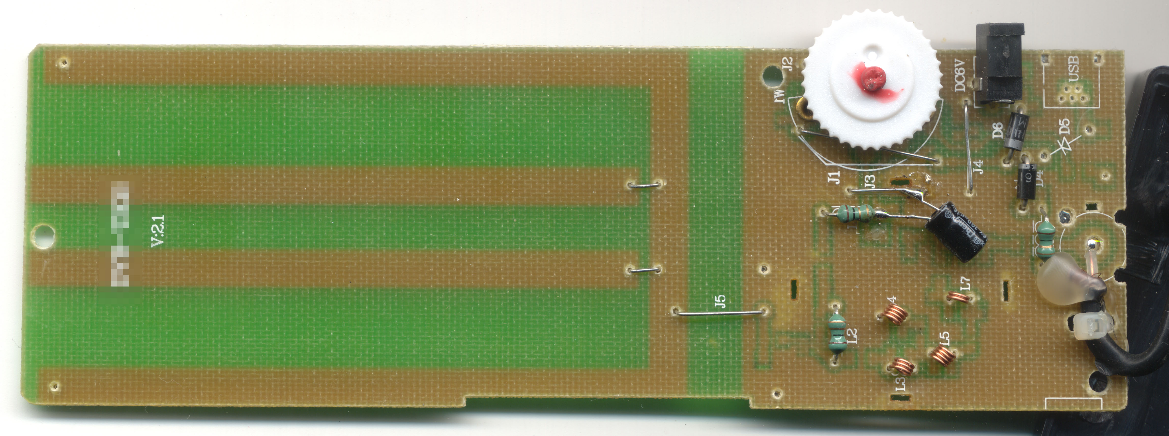
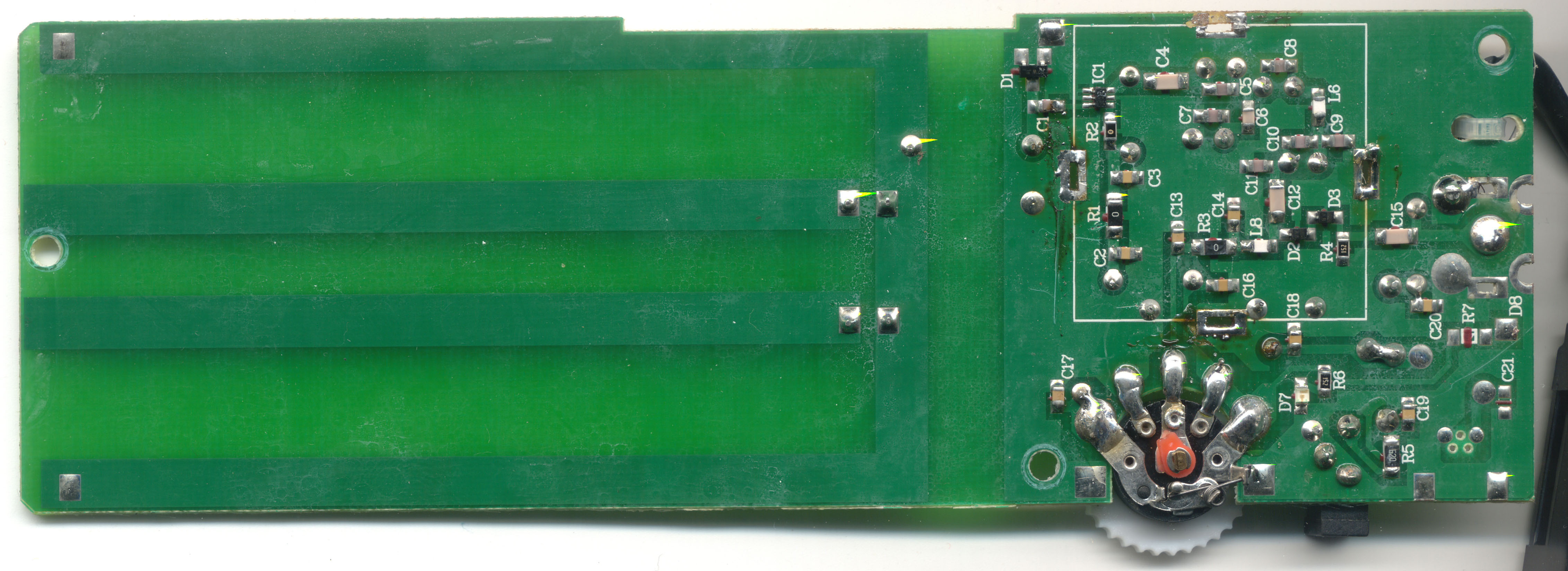
The Ware for May 2015 is a DVB antenna amplifier. The brand/model number is Draco-HDT2-7300. Lots of excellent submissions and in an act of total arbitrary judgment I’ll say pelrun is the winner for calling it as an amplified TV antenna first. Gratz, email me for your prize!
Winner, Name that Ware May 2015
July 1st, 2015Name that Ware, May 2015
May 30th, 2015The Ware for May 2015 is below.
Thanks to xobs for contributing this ware!
Winner, Name that Ware April 2015
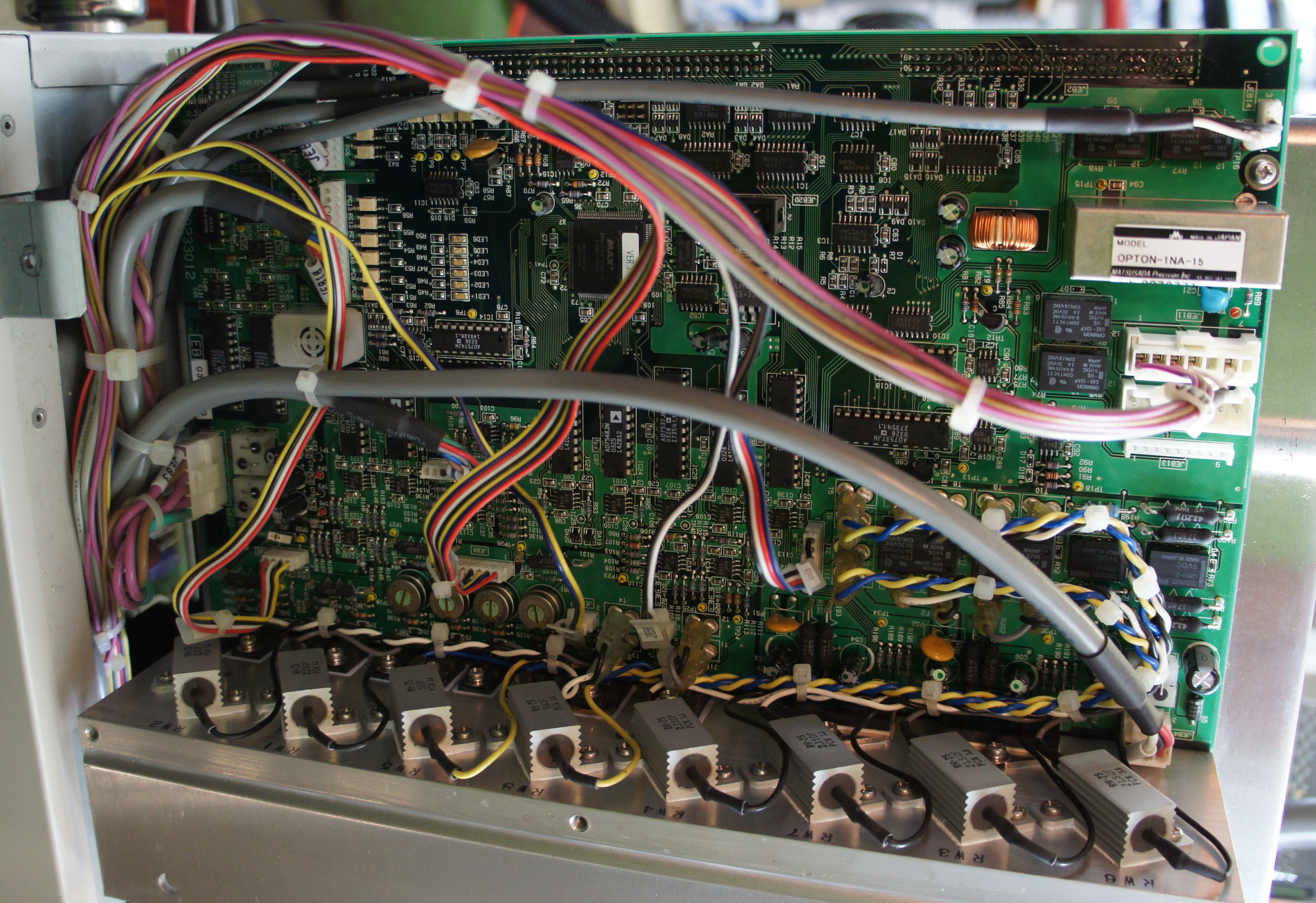
May 30th, 2015The Ware for April 2015 is a control board from a Keyence VE-7800 SEM, which I bought with some friends for a steal at a used equipment shop. Unlike my previous SEM adventure, this one is in good working order.
Nobody guessed it correctly, but I liked Dave Z’s analysis, and also Paul Campbell’s comment about two engineers at war. It’s a nice mental image :) However, the fact that Christian Vogel picked up on the vacuum flange in the background, that was really subtle, so I’ll declare him the winner. Gratz, email me for your prize!
Name that Ware April 2015
April 28th, 2015The Ware for April 2015 is shown below.
Have fun!
Winner, Name that Ware March 2015
April 28th, 2015The Ware for March 2015 is a PC AT Single T4 4 Meg Transputer board assembly. Jim is the winner, congrats! Email me to claim your prize.